martes, 16 de febrero de 2010

Noise figure (NF)
is a measure of degradation of the signal-to-noise ratio (SNR), caused by components in a radio frequency (RF) signal chain. The noise figure is defined as the ratio of the output noise power of a device to the portion thereof attributable to thermal noise in the input termination at standard noise temperature T0 (usually 290 K). The noise figure is thus the ratio of actual output noise to that which would remain if the device itself did not introduce noise. It is a number by which the performance of a radio receiver can be specified.
The noise figure is the difference in decibels (dB) between the noise output of the actual receiver to the noise output of an “ideal” receiver with the same overall gain and bandwidth when the receivers are connected to sources at the standard noise temperature T0 (usually 290 K). The noise power from a simple load is equal to kTB, where k is Boltzmann's constant, T is the absolute temperature of the load (for example a resistor), and B is the measurement bandwidth.
This makes the noise figure a useful figure of merit for terrestrial systems where the antenna effective temperature is usually near the standard 290 K. In this case, one receiver with a noise figure say 2 dB better than another, will have an output signal to noise ratio that is about 2 dB better than the other. However, in the case of satellite communications systems, where the antenna is pointed out into cold space, the antenna effective temperature is often colder than 290 K. In these cases a 2 dB improvement in receiver noise figure will result in more than a 2 dB improvement in the output signal to noise ratio. For this reason, the related figure of effective noise temperature is therefore often used instead of the noise figure for characterizing satellite-communication receivers and low noise amplifiers.
In heterodyne systems, output noise power includes spurious contributions from image-frequency transformation, but the portion attributable to thermal noise in the input termination at standard noise temperature includes only that which appears in the output via the principal frequency transformation of the system and excludes that which appears via the image frequency transformation.

Definition

The noise factor of a system is defined as:
F = \frac{\mathrm{SNR}_\mathrm{in}}{\mathrm{SNR}_\mathrm{out}}
where SNRin and SNRout are the input and output power signal-to-noise ratios, respectively. The noise figure is defined as:
NF = 10 \log\left(\frac{\mathrm{SNR}_\mathrm{in}}{\mathrm{SNR}_\mathrm{out}}\right) = \mathrm{SNR}_\mathrm{in, dB} - \mathrm{SNR}_\mathrm{out, dB}
where SNRin,dB and SNRout,dB are in decibels (dB). The noise figure is the noise factor, given in dB:
NF = 10 \log \left(F\right)
These formulae are only valid when the input termination is at standard noise temperature T0, although in practice small differences in temperature do not significantly affect the values.
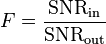
The noise factor of a device is related to its noise temperature Te:
F = 1 + \frac{T_e}{T_0}
Devices with no gain (e.g., attenuators) have a noise figure equal to their attenuation L (absolute value, not in dB) when their physical temperature equals T0. More generally, for an attenuator at a physical temperature T, the noise temperature is Te = (L − 1)T, giving a noise factor of:
F = 1 + \frac{(L-1)T}{T_0}
If several devices are cascaded, the total noise factor can be found with Friis' Formula:
F = F_1 + \frac{F_2 - 1}{G_1} + \frac{F_3 - 1}{G_1  G_2} + \frac{F_4 - 1}{G_1 G_2 G_3} + \cdots + \frac{F_n - 1}{G_1 G_2 G_3 \cdots G_{n-1}},
where Fn is the noise factor for the n-th device and Gn is the power gain (linear, not in dB) of the n-th device. In a well designed receive chain, only the noise factor of the first amplifier should be significant.

Rooselvet Ramirez    CAF

Amplificador diferencial

Se llama amplificador diferencial a un amplificador cuya salida es proporcional a la diferencia entre sus dos entradas (Vi+ y Vi-). La salida puede ser diferencial o no, pero en ambos casos, referida a masa.

Tecnología


Amplificador diferencial
El amplificador diferencial (o par diferencial) suele construirse con dos transistores que comparten la misma conexión de emisor, por la que se inyecta una corriente de polarización. Las bases de los transistores son las entradas (I+ e I-), mientras que los colectores son las salidas. Si se terminan en resistencias, se tiene una salida también diferencial. Se puede duplicar la ganancia del par con un espejo de corriente entre los dos colectores.
Aunque esta descripción se basa en transistores de unión bipolar, lo mismo se puede hacer en tecnología MOS ó CMOS.

Aplicaciones

El par diferencial es una base fundamental para la electrónica analógica. Los amplificadores operacionales y comparadores de tensión se basan en él. Así mismo, los multiplicadores analógicos, empleados en calculadoras analógicas y en mezcladores, están basados en pares diferenciales.
Los amplificadores de transconductancia también, básicamente, son pares diferenciales.
En electrónica digital, la tecnología ECL se basa en un par diferencial. Muchos circuitos de interfaz y cambiadores de nivel se basan en pares diferenciales.

Rooselvet Ramirez        EES
Models for device design
The modern transistor has an internal structure that exploits complex physical mechanisms. Device design requires a detailed understanding of how device manufacturing processes such as ion implantation, impurity diffusion, oxide growth, annealing, and etching affect device behavior. Process models simulate the manufacturing steps and provide a microscopic description of device "geometry" to the device simulator. By "geometry" is meant not only readily identified geometrical features such as whether the gate is planar or wrap-around, or whether the source and drain are raised or recessed (see Figure 1 for a memory device with some unusual modeling challenges related to charging the floating gate by an avalanche process), but also details inside the structure, such as the doping profiles after completion of device processing.

Figure 1: Floating-gate avalanche injection memory device FAMOS
With this information about what the device looks like, the device simulator models the physical processes taking place in the device to determine its electrical behavior in a variety of circumstances: DC current-voltage behavior, transient behavior (both large-signal and small-signal), dependence on device layout (long and narrow versus short and wide, or interdigitated versus rectangular, or isolated versus proximate to other devices). These simulations tell the device designer whether the device process will produce devices with the electrical behavior needed by the circuit designer, and is used to inform the process designer about any necessary process improvements. Once the process gets close to manufacture, the predicted device characteristics are compared with measurement on test devices to check that the process and device models are working adequately.
Although long ago the device behavior modeled in this way was very simple - mainly drift plus diffusion in simple geometries - today many more processes must be modeled at a microscopic level; for example, leakage currents in junctions and oxides, complex transport of carriers including velocity saturation and ballistic transport, quantum mechanical effects, use of multiple materials (for example, Si-SiGe devices, and stacks of different dielectrics) and even the statistical effects due to the probabilistic nature of ion placement and carrier transport inside the device. Several times a year the technology changes and simulations have to be repeated. The models may require change to reflect new physical effects, or to provide greater accuracy. The maintenance and improvement of these models is a business in itself.
These models are very computer intensive, involving detailed spatial and temporal solutions of coupled partial differential equations on three-dimensional grids inside the device.[1] [2] [3] [4] [5] Such models are slow to run and provide detail not needed for circuit design. Therefore, faster transistor models oriented toward circuit parameters are used for circuit design.

Models for circuit design (compact models)

Transistor models are used for almost all modern electronic design work. Analog circuit simulators such as SPICE use models to predict the behavior of a design. Most design work is related to integrated circuit designs which have a very large tooling cost, primarily for the photomasks used to create the devices, and there is a large economic incentive to get the design working without any iterations. Complete and accurate models allow a large percentage of designs to work the first time.
Modern circuits are usually very complex. The performance of such circuits is difficult to predict without accurate computer models, including but not limited to models of the devices used. The device models include effects of transistor layout: width, length, interdigitation, proximity to other devices; transient and DC current-voltage characteristics; parasitic device capacitance, resistance, and inductance; time delays; and temperature effects; to name a few items. [6]

 Large-signal nonlinear models

Nonlinear, or large signal transistor models fall into three main types:[7][8]

 Physical models

These are models based upon device physics, based upon approximate modeling of physical phenomena within a transistor. Parameters within these models are based upon physical properties such as oxide thicknesses, substrate doping concentrations, carrier mobility, etc. In the past these models were used extensively, but the complexity of modern devices makes them inadequate for quantitative design. Nonetheless, they find a place in hand analysis (that is, at the conceptual stage of circuit design), for example, for simplified estimates of signal-swing limitations.

 Empirical models

This type of model is entirely based upon curve fitting, using whatever functions and parameter values most adequately fit measured data to enable simulation of transistor operation. Unlike a physical model, the parameters in an empirical model need have no fundamental basis, and will depend on the fitting procedure used to find them. The fitting procedure is key to success of these models if they are to be used to extrapolate to designs lying outside the range of data to which the models were originally fitted. Such extrapolation is a hope of such models, but is not fully realized so far.

 Tabular models

The third type of model is a form of look-up table containing a large number of values for common device parameters such as drain current and device parasitics. These values are indexed in reference to their corresponding bias voltage combinations. Thus, model accuracy is increased by inclusion of additional data points within the table. The chief advantage of this type of model is decreased simulation time (see article look-up table for discussion of the computational advantages of look-up tables). A limitation of these models is that they work best for designs that use devices within the table (interpolation) and are unreliable for devices outside the table (extrapolation).
The use of nonlinear models, which describe the entire operating area of a transistor, is required for digital designs, for circuits that operate in a large-signal regime such as power amplifiers and mixers, and for the large-signal simulation of any circuit, for example, for stability or distortion analysis.
Nonlinear models are used with a computer simulation program, such as SPICE. The models in SPICE are a hybrid of physical and empirical models, and such models are incomplete unless they include specification of how parameter values are to be extracted, especially as "unrealistic" (that is, unphysical) values can be made to fit the measured data without such a prescription. An incorrect set of fitting parameters results in wild predictions for devices that were not part of the originally fitted data set.
Large-signal computer models for devices continually evolve to keep up with changes in technology. To attempt standardization of model parameters used in different simulators, an industry working group was formed, the Compact Model Council, to choose, maintain and promote the use of standard models. An elusive goal in such modeling is prediction of how circuits using the next generation of devices should work, to identify before the next step which direction the technology should take, and have models ready beforehand.
Rooselvet Ramirez        EES
In electronics, a common-base (also known as grounded-base) amplifier is one of three basic single-stage bipolar junction transistor (BJT) amplifier topologies, typically used as a current buffer or voltage amplifier. In this circuit the emitter terminal of the transistor serves as the input, the collector the output, and the base is common to both (for example, it may be tied to ground reference or a power supply rail), hence its name. The analogous field-effect transistor circuit is the common-gate amplifier.

Figure 1: Basic NPN common-base circuit (neglecting biasing details).
Applications
This arrangement is not very common in low-frequency circuits, where it is usually employed for amplifiers that require an unusually low input impedance, for example to act as a preamplifier for moving-coil microphones. However, it is popular in high-frequency amplifiers, for example for VHF and UHF, because its input capacitance does not suffer from the Miller effect, which degrades the bandwidth of the common-emitter configuration, and because of the relatively high isolation between the input and output. This high isolation means that there is little feedback from the output back to the input, leading to high stability.
This configuration is also useful as a current buffer since it has a current gain of approximately unity (see formulas below). Often a common base is used in this manner, preceded by a common-emitter stage. The combination of these two form the cascode configuration, which possesses several of the benefits of each configuration, such as high input impedance and isolation.
Overview of characteristics
Several example applications are described in detail below. A brief overview follows.
  • The amplifier input impedance Rin looking into the emitter node is very low, given approximately by
 R_{in} = r_E =  \begin{matrix} \frac {V_T} {I_E} \end{matrix}  ,
where VT is the thermal voltage and IE is the DC emitter current.
For example, for VT = 26 mV and IE = 10 mA, rather typical values, Rin = 2.6 Ω. If IE is reduced to increase Rin, there are other consequences like lower transconductance, higher output resistance and lower β that also must be considered. A practical solution to this low-input-impedance problem is to place a common-emitter stage at the input to form a cascode amplifier.
  • Because the input impedance is so low, most signal sources have larger source impedance than the common-base amplifier Rin. The consequence is that the source delivers a current to the input rather than a voltage, even if it is a voltage source. (According to Norton's theorem, this current is approximately iin = vS / RS). If the output signal also is a current, the amplifier is a current buffer and delivers the same current as is input. If the output is taken as a voltage, the amplifier is a transresistance amplifier, and delivers a voltage dependent on the load impedance, for example vout = iin RL for a resistor load RL much smaller in value than the amplifier output resistance Rout. That is, the voltage gain in this case (explained in more detail below) is:
 v_{out} = i_{in} R_L = v_s \begin{matrix} \frac {R_L}{R_S} \end{matrix} \ \ \rarr A_v =\begin{matrix}\frac {v_{out}}{v_{S}} = \frac {R_L}{R_S} \end{matrix} .
Note for source impedances such that RS >> rE the output impedance approaches Rout = RC || [ gm ( rπ || RS ) rO ].
  • For the special case of very low impedance sources, the common-base amplifier does work as a voltage amplifier, one of the examples discussed below. In this case (explained in more detail below), when RS << rE and RL << Rout, the voltage gain becomes:
A_v =\begin{matrix}\frac {v_{out}}{v_{S}} = \frac {R_L}{r_E} \approx g_m R_L\end{matrix} ,
where gm = IC / VT is the transconductance. Notice that for low source impedance, Rout = rO || RC.
  • The inclusion of rO in the hybrid-pi model predicts reverse transmission from the amplifiers output to its input, that is the amplifier is bilateral. One consequence of this is that the input/output impedance is affected by the load/source termination impedance, hence, for example, the output resistance, Rout, may vary over the range rO || RC ≤ Rout ≤ (β + 1) rO || RC depending on the source resistance, RS. The amplifier can be approximated as unilateral when neglect of rO is accurate (valid for low gains and low to moderate load resistances), simplifying the analysis. This approximation often is made in discrete designs, but may be less accurate in RF circuits, and in integrated circuit designs where active loads normally are used.
Rooselvet Ramirez        EES

lunes, 15 de febrero de 2010

Common-emitter amplifiers give the amplifier an inverted output and can have a very high gain and can vary widely from one transistor to the next. The gain is a strong function of both temperature and bias current, and so the actual gain is somewhat unpredictable. Stability is another problem associated with such high gain circuits due to any unintentional positive feedback that may be present. Other problems associated with the circuit are the low input dynamic range imposed by the small-signal limit; there is high distortion if this limit is exceeded and the transistor ceases to behave like its small-signal model. One common way of alleviating these issues is with the use of negative feedback, which is usually implemented with emitter degeneration. Emitter degeneration refers to the addition of a small resistor (or any impedance)[disambiguation needed] between the emitter and the common signal source (e.g., the ground reference or a power supply rail). This impedance RE reduces the overall transconductance Gm = gm of the circuit by a factor of gmRE + 1, which makes the voltage gain
A_{\text{v}} \triangleq \frac{ v_{\text{out}} }{ v_{\text{in}} } = \frac{ -g_m R_{\text{C}} }{ g_m R_{\text{E}}+1 } \approx -\frac{ R_{\text{C}} }{ R_{\text{E}} } \qquad (\text{where} \quad g_m R_{\text{E}} \gg 1). \,
So the voltage gain depends almost exclusively on the ratio of the resistors RC / RE rather than the transistor's intrinsic and unpredictable characteristics. The distortion and stability characteristics of the circuit are thus improved at the expense of a reduction in gain.

Figure 2: Adding an emitter resistor decreases gain, but increases linearity and stability
Characteristics
At low frequencies and using a simplified hybrid-pi model, the following small-signal characteristics can be derived.
If the emitter degeneration resistor is not present, R_{\text{E}} = 0\,\Omega. As expected, when R_{\text{E}}\, is increased, the input impedance is increased and the voltage gain A_{\text{v}}\, is reduced.

[edit] Bandwidth

The bandwidth of the common-emitter amplifier tends to be low due to high capacitance resulting from the Miller effect. The parasitic base-collector capacitance C_{\text{CB}}\, appears like a larger parasitic capacitor C_{\text{CB}} (1-A_{\text{v}})\, (where A_{\text{v}}\, is negative) from the base to ground[1]. This large capacitor greatly decreases the bandwidth of the amplifier as it makes the time constant of the parasitic input RC filter r_{\text{s}} (1-A_{\text{V}}) C_{\text{CB}}\, where r_{\text{s}}\, is the output impedance of the signal source connected to the ideal base.
The problem can be mitigated in several ways, including:
The Miller effect negatively affects the performance of the common-source amplifier in the same way (and has similar solutions).

Rooselvet Ramirez     EES
Una red de dos puertos (una especie de red de cuatro terminales o quadripole) es un circuito eléctrico o un dispositivo con dos pares de terminales conectadas internamente por una red eléctrica. Two terminals constitute a port if they satisfy the essential requirement known as the port condition : the same current must enter and leave a port. [ 1 ] [ 2 ] Dos terminales constituyen un puerto, si cumplen los requisitos esenciales se conoce como la condición de puerto: la misma corriente debe entrar y salir de un puerto. [1] [2]
Examples include small-signal models for transistors (such as the hybrid-pi model ), filters and matching networks . Los ejemplos incluyen los modelos de pequeña señal para transistores (como el modelo híbrido-pi), filtros y redes de adaptación. The analysis of passive two-port networks is an outgrowth of reciprocity theorems first derived by Lorentz [ 3 ] . El análisis de dos redes de puertos pasivos-es una consecuencia de la reciprocidad teoremas primera obtenidos por Lorenz [3].
A two-port network makes possible the isolation of either a complete circuit or part of it and replacing it by its characteristic parameters. Una red de dos puertos que hace posible el aislamiento de un circuito ya sea completo o parte de ella y su sustitución por los parámetros característicos. Once this is done, the isolated part of the circuit becomes a " black box " with a set of distinctive properties, enabling us to abstract away its specific physical buildup, thus simplifying analysis. Una vez hecho esto, la parte aislada del circuito se convierte en un "recuadro negro" con un conjunto de propiedades distintivas, que nos permite abstraer su acumulación física específica, lo que simplifica el análisis. Any linear circuit with four terminals can be transformed into a two-port network provided that it does not contain an independent source and satisfies the port conditions. Cualquier circuito lineal con cuatro terminales se puede transformar en una red de dos puertos siempre que no contiene una fuente independiente y cumple las condiciones del puerto.
There are a number of alternative sets of parameters that can be used to describe a linear two-port network, the usual sets are respectively called z , y , h , g , and ABCD parameters, each described individually below. Hay una serie de conjuntos alternativos de los parámetros que se pueden utilizar para describir dos lineales de redes portuarias, los conjuntos de costumbre son, respectivamente, denominada Z, Y, H, G, y los parámetros ABCD, explica cada uno individualmente a continuación. These are all limited to linear networks since an underlying assumption of their derivation is that any given circuit condition is a linear superposition of various short-circuit and open circuit conditions. Todos estos son limitados a redes lineales desde un supuesto subyacente de su obtención es que cualquier condición de circuito determinado es una superposición lineal de varios de corto-circuito y las condiciones de circuito abierto. They are usually expressed in matrix notation, and they establish relations between the variables Por lo general son expresados en notación matricial, y establecer relaciones entre las variables
V_ (1) \, \ stackrel (\ text (def }}{=} \ () Input voltage Tensión de entrada
V_ (2) \, \ stackrel (\ text (def }}{=} \ () Output voltage Tensión de salida
I_ (1) \, \ stackrel (\ text (def }}{=} \ () Input current Corriente de entrada
I_ (2) \, \ stackrel (\ text (def }}{=} \ () Output current Corriente de salida
which are shown in Figure 1. la que se muestran en la Figura 1. These current and voltage variables are most useful at low-to-moderate frequencies. Estas variables actuales y la tensión son muy útiles en baja a frecuencias moderadas. At high frequencies (eg, microwave frequencies), the use of power and energy variables is more appropriate, and the two-port current–voltage approach is replaced by an approach based upon scattering parameters . A altas frecuencias (por ejemplo, las frecuencias de microondas), el uso de la energía y las variables de la energía es más apropiado, y los dos puertos de tensión actual enfoque se sustituye por un enfoque basado en los parámetros de dispersión.
The terms four-terminal network and quadripole (not to be confused with quadrupole ) are also used, the latter particularly in more mathematical treatments although the term is becoming archaic. Los términos de red de cuatro terminales y quadripole (no debe confundirse con cuadrupolo) también se utilizan, estos últimos especialmente en tratamientos más matemática, aunque el término es cada vez arcaica. However, a pair of terminals can be called a port only if the current entering one terminal is equal to the current leaving the other; this definition is called the port condition . Sin embargo, un par de terminales puede ser llamado un puerto sólo si la corriente de entrada de un terminal es igual a la corriente que sale del otro; esta definición se llama la condición de puerto. A four-terminal network can only be properly called a two-port when the terminals are connected to the external circuitry in two pairs both meeting the port condition. [ 1 ] [ 2 ] Una red de cuatro terminales sólo puede hablarse de un doble puerto cuando los terminales están conectados a los circuitos externos en los dos pares que cumplen la condición de puerto.

Figure 1: Example two-port network with symbol definitions. Figura 1: Ejemplo de red de dos puertos con las definiciones de símbolos. Notice the port condition is satisfied: the same current flows into each port as leaves that port. Notificación de la condición de puerto se cumple: los flujos de la misma corriente en cada puerto, las hojas de ese puerto.
Parámetros de impedancia (Z-parámetros)

Figure 2: z-equivalent two port showing independent variables I 1 and I 2 . Figura 2: Z-dos equivalente puerto mostrando variables independientes I 1 y 2. Although resistors are shown, general impedances can be used instead. Aunque se muestran resistencias, impedancias general se pueden utilizar en su lugar.
Main article: Impedance parameters Artículo principal: parámetros de impedancia
\ begin (bmatrix) V_1 \ \ V_2 \ end (bmatrix) = \ begin (bmatrix z_) (11) & z_ (12) \ \ Z_ (21) & z_ (22) \ end (bmatrix) \ begin (bmatrix) \ I_1 \ I_2 \ end (bmatrix)
where dónde
Z_ (11) \, \ stackrel (\ text (def }}{=} \ \ left. \ frac (V_1) (I_1) \ right | _ (I_2 = 0) \ qquad Z_ (12) \, \ stackrel (\ text (def }}{=} \, \ left. \ frac (V_1) (I_2) \ right | _ (I_1 = 0)
Z_ (21) \, \ stackrel (\ text (def }}{=} \ \ left. \ frac (V_2) (I_1) \ right | _ (I_2 = 0) \ qquad Z_ (22) \, \ stackrel (\ text (def }}{=} \, \ left. \ frac (V_2) (I_2) \ right | _ (I_1 = 0)
Notice that all the z-parameters have dimensions of ohms . Observe que todos los parámetros z tienen dimensiones de ohmios.
For reciprocal networks Para las redes de reciprocidad \ textstyle Z_ (12) = Z_ (21) . . For symmetrical networks Para las redes simétricas \ textstyle Z_ (11) = Z_ (22) . . For lossless networks all the Para las redes sin pérdida de todos los \ textstyle z_ \ mathrm (min) are purely imaginary.  son puramente imaginarios.
Rooselvet Ramirez    EES