Mostrando entradas con la etiqueta 1II 2010-1 CAF Freddy Vallenilla. Mostrar todas las entradas

domingo, 25 de julio de 2010

A Step Towards Germanium Nanoelectronics


The use of germanium instead of silicon as basic material of transistors would enable faster chips containing smaller transistors. However, a number of problems still have to be solved.


The figure shows schematically the application of germanium in a CMOS (complementary metal oxide semiconductor) circuit. Note that germanium is only used in the regions of source (S), drain (D) and channel (C). Source and drain contain high concentration of foreign atoms (dopants) which provide the excess of free electrons (n+ regions) or holes (p+ regions)

Transistors are produced using foreign atoms that are implanted into the semiconductor material so that it becomes partly conducting. As this production step damages the material, it has to be repaired by subsequent annealing. So far it has not been possible to produce large-scale integrated transistors of a specific type (NMOS) using germanium. The reason: phosphorus atoms are strongly redistributed within the material during annealing.

Two novel techniques, which were applied by scientists of the research center Forschungszentrum Dresden-Rossendorf (FZD) and international colleagues, overcome this dilemma.

Higher switching speeds than in silicon could be achieved using germanium and some other semiconductors. Germanium is particularly attractive since it could be easily integrated into existing technological processes. Germanium was the basic material of first-generation transistors before it was replaced by silicon at the end of the 1960s. This was due to the excellent electronic properties of the interface between the semiconductor silicon and its insulating and passivating oxide. However, this advantage cannot be utilized if transistor dimensions are further reduced since the oxide must then be replaced by so-called high-k dielectrics. This again stimulates science and industry to search for the most suitable basic material.

By inserting foreign atoms the conductivity of semiconductors can be varied in a purposeful way. One possibility is ion implantation (ions are charged atoms) with subsequent heat treatment, which is called annealing. Annealing of the germanium crystal is necessary as the material is heavily damaged during implantation, and leads to the requested electronic properties. While these methods allow for the manufacturing of p-channel transistors (PMOS) according to future technology needs (22 nanometer technology node), it was not possible to produce corresponding n-channel transistors (NMOS) using germanium. This is due to the strong spatial redistribution (diffusion) of the phosphorus atoms which have to be used in manufacturing the n+ regions.

Physicists from the FZD applied a special annealing method that enables repairing the germanium crystal and yields good electrical properties without the diffusion of phosphorus atoms. The germanium samples were heated by short light pulses of only a few milliseconds. This period is sufficient in order to restore the crystal quality and to achieve electrical activation of phosphorus, but it is too short for the spatial redistribution of the phosphorus atoms. The light pulses were generated by the flash lamp equipment which was developed at the research center FZD. Analysis of the electrical and structural properties of the thin phosphorus-doped layers in germanium was performed in close collaboration with colleagues from the Belgian microelectronics center IMEC in Leuven and from the Fraunhofer-Center for Nanoelectronic Technologies (CNT) in Dresden.

An alternative method to suppress phosphorus diffusion in germanium has been investigated by an international team consisting of researchers from Germany, Denmark and the USA, amongst them physicists from FZD. After ion implantation of phosphorus into germanium the sample was heated to a given temperature and then irradiated by protons. It could be demonstrated that this treatment leads to the reduction of phosphorus diffusion, too. The results of these experiments are explained by the influence of certain lattice defects (self-interstitials) that annihilate those lattice defects (vacancies) which are responsible for the mobility of the phosphorus atoms.

Thus, FZD physicists and their colleagues demonstrated that in principle it is possible to fabricate germanium-based n-channel transistors (NMOS) with dimensions corresponding to the most advanced technological requirements.


Freddy Vallenilla, CAF

Fast Transistors Could Save Energy


Transistors, the cornerstone of electronics, are lossy and therefore consume energy. Researchers from the ETH Zürich and EPF Lausanne have developed transistors targeting high switching speeds and higher output powers. The devices can be used more efficiently as conventional transistors, so as to reduce energy consumption and CO2 emissions.


Gate electrode of an AlInN/GaN HEMT (High Electron Mobility Transistor)

They consist of complex structures, some of which are only a few nanometers in size, and can be found in most electronic networks: transistors built from semiconductor materials deposited on a supporting substrate such as silicon carbide (SiC). Colombo Bolognesi, Professor for Millimeter-Wave Electronics at the ETH Zürich, and his research group specialize in developing high-performance transistors intended to transmit information as quickly and efficiently as possible. In order to do this, electrons must move through the semiconductor material as fast as possible. Just last year, Bolognesi`s group improved its own speed record for so-called "High Electron Mobility Transistors (HEMTs)" based on Aluminium-Gallium Nitride (AlGaN/GaN) materials depossited on Silicon substrates. Before then, comparable technologies showed cutoff frequencies of 28 Gigahertz (GHz), but devices built by Bolognesi`s Group in the FIRST cleanroom reached cutoff frequencies as high as 108 GHz.

New Material

Bolognesi's team, now in collaboration with the group of Nicolas Grandjean (who is a Professor of Physics at the EPF Lausanne) also explores a new material: instead of using Aluminium-Gallium Nitride, the researchers exploit the favorable properties of a newer material combination consisting of Alumimium Indium Nitride (AlInN/GaN). The advantage here is that AlInN has a significantly larger "forbidden energy gap" than other commonly used semiconductors. The so-called forbidden energy gap is one of the most important properties of a semiconductor material.

Semiconductors featuring a large energy gap can be used to build transistors which operate at much higher temperatures, sustain greater voltage levels, and handle higher signal power levels than possible with smaller gap conventional materials such as Silicon. "Other researchers have already demonstrated that AlInN/GaN HEMT transistors can operate at temperatures as high as 1000 C -- that far exceeds the capabilities of Silicon and even AlGaN/GaN transistors," says Bolognesi.

Until now, AlInN/GaN transistors were however slower than their AlGaN/GaN counterparts. The researchers have now eliminated this problem. They managed to break their own record of 102 GHz, achieved with AlInN/GaN transistors built on Silicon, with an AlInN/GaN transistor built on a Silicon Carbide substrate. In a single step, they increased the cutoff frequency by 41 percent up to 144 GHz. "That is a huge improvement," states Bolognesi with delight. "Imagine for example a sprinter who would suddenly run the hundred meter 40 percent faster." And fresh from the laboratory, as this article is being written, Bolognesi reports that his team just measured cutoff frequencies as high as 200 GHz. "That shatters all records in this research field."

Significant decrease in energy consumption

One possible commercial application of similar transistors could be in the power amplifiers driving wireless transmitter antennaes. There, Gallium Nitride transistors would help reduce energy costs thanks to their higher efficiency. For example, "a mobile phone operator with 10'000 base stations equipped with conventional power amplifiers consumes on average 30 Megawatt each year, with associated CO2 emissions of 100'000 tons," says Bolognesi. "Roughly 80 percent of that energy is just wasted as heat, and even more if the transmitter equipment must be air conditioned."

By using Gallium Nitride transistors, mobile telephone operators could significantly decrease their energy consumption, and reduce their CO2 emissions by several tens of thousand tons. Note that 10'000 tons of CO2 corresponds to the CO2 emission from 5'000 mid-class automobiles driven for 10'000 kilometers per year. For reference, there is roughly 11'000 wireless base stations currently operating throughout Switzerland.

Bolognesi believes Gallium Nitride based transistors could improve wireless transmitter efficiencies from 15 to 20 percent today, up to 60 percent. The researcher credits the group`s outstanding results to his team`s process know-how and dedication, the outstanding FIRST Laboratory facilities, as well as to the quality of the materials supplied by his EPFL collaborators. Encouraged by their recent achievements, the researchers continue to work with great enthusiam to further stretch the envelope of transistor performances.


Freddy Vallenilla, CAF

Single-Atom Transistor Discovered


Researchers from Helsinki University of Technology (Finland), University of New South Wales (Australia), and University of Melbourne (Australia) have succeeded in building a working transistor, whose active region composes only of a single phosphorus atom in silicon.

(a) Colored scanning electron microscope image of the measured device. Aluminum top gate is used to induce a two-dimensional electron layer at the silicon-silicon oxide interface below the metallization. The barrier gate is partially below the top gate and depletes the electron layer in the vicinity of the phosphorus donors (the red spheres added to the original image). The barrier gate can also be used to control the conductivity of the device. All the barrier gates in the figure form their own individual transistors. (b) Measured differential conductance through the device at 4 Tesla magnetic field. The red and the yellow spheres illustrate the spin-down and -up states of a donor electron which induce the lines of high conductivity clearly visible in the figure. (Credit: American Chemical Society)

The results have just been published in Nano Letters, a journal of the American Chemical Society.
The working principles of the device are based on sequential tunneling of single electrons between the phosphorus atom and the source and drain leads of the transistor. The tunneling can be suppressed or allowed by controlling the voltage on a nearby metal electrode with a width of a few tens of nanometers.
The rapid development of computers, which created the present information society, has been mainly based on the reduction of the size of transistors. Scientists have known for a long time that this development has to slow down critically during the future decades when the even tighter inexpensive packing of transistors would require them to shrink down to the atomic length scales. In the recently developed transistor, all the electric current passes through the same single atom. This allows researchers to study the effects arising in the extreme limit of the transistor size.
"About half a year ago, I and one of the leaders of this research, Prof. Andrew Dzurak, were asked when we expect a single-atom transistor to be fabricated. We looked at each other, smiled, and said that we have already done that," says Dr. Mikko Möttönen. "In fact, our purpose was not to build the tiniest transistor for a classical computer, but a quantum bit which would be the heart of a quantum computer that is being developed worldwide," he continues.
Problems arising when the size of a transistor is shrunk towards the ultimate limit are due to the emergence of so-called quantum mechanical effects. On one hand, these phenomena are expected to challenge the usual transistor operation. On the other hand, they allow classically irrational behavior which can, in principle, be harnessed for conceptually more efficient computing, quantum computing.
The driving force behind the measurements reported now is the idea to utilize the spin degree of freedom of an electron of the phosphorus donor as a quantum bit, a qubit. The researchers were able to observe in their experiments spin up and down states for a single phosphorus donor for the first time. This is a crucial step towards the control of these states, that is, the realization of a qubit.


Freddy Vallenilla, CAF

Flaw revealed in theory of transistor 'noise'


Engineers in the US and Taiwan have carried out an experiment that they say exposes a serious flaw in our understanding of how transistors work. The research finds that as transistors shrink, the amplitude of electronic "noise" in these devices grows even more than standard theory says it should. The researchers warn that unless our understanding of noise is reviewed, then development of next-generation laptops, mobile phones and other low-power devices could be hampered.
Transistors perform an essential role in electronic devices by amplifying and switching signals, but in order to do this reliably they must be made from highly purified materials. Defects in these materials can — like rocks in a stream — impede the flow of current and cause a transistor to malfunction. As a result, the transistor may fluctuate rapidly between its "on" and "off" states in an effect known as "random telegraph noise".

What's all that noise about?
For decades, engineers have been guided by a standard theory that says these fluctuations should become larger as transistors get ever smaller in size, spelling bad news for low-power devices. Recent findings from Kin Cheung and colleagues of the National Institute of Standards and Technology (NIST) in Gaithersburg have shown that the fluctuations may be somewhat larger than predicted and, more importantly, the frequency of their occurrence is inconsistent with conventional noise theories.
These researchers looked specifically at the most common transistor in both digital and analogue circuits — the MOSFET, or the metal–oxide–semiconductor field-effect transistor. Surprisingly, they found that even in nanoscale transistors with widths and lengths of 0.085 micrometres and 0.055 micrometres, the frequency at which the device fluctuates between on and off states does not vary much from larger transistors.
Whilst there have been previous criticisms of the standard model for noise, no-one has been able to prove unequivocally that it is flawed. Cheung and his team now say their results are the most convincing falsifier yet because they have been generated using an "ultra-thin" transistor. With the gate dielectric being only a few molecules thick, they claim they can rule out other potential sources of noise and showcase the first "absolute test" of the standard theory. "We have now used our data to examine all the alternative models and found that, to first order, none of them work,"

It's good to talk
If the current model of noise is indeed wrong then this could have a significant impact on the design of low-power technologies. The hope is that consumers will see benefits like mobile phones that can run for a week on a single charge or pacemakers that operate for a decade without requiring a change of batteries. These would require very small and reliable transistors. "We have to understand the problem before we can fix it — and troublingly, we don't know what's actually happening," said Jason Campbell, another of the NIST researchers.
Asen Asenov, an electronics researcher at the University of Glasgow in the UK believes this research addresses a pressing issue in electronics. "RTN has become dramatically important and is a main show stopper to the Flash memory scaling," he said. Asenov is concerned, however, that the researchers do not take into account that transistors occasionally capture single electrons. "[electron capture] creates localized depletion regions in the semiconductor changing the relative position of the energy level and the conduction band."
Even though Cheung and his team have taken these accurate readings, physicists will now need to carry out more research in order to confirm what is really going on in ultra-small transistors.


Freddy Vallenilla, CAF

Graphene transistor breaks new record


Graphene FET hits 100 GHz
Physicists in the US have made the fastest graphene transistor ever, with a cut-off frequency of 100 GHz. The device can be further miniaturized and optimized so that it could soon outperform conventional devices made from silicon, says the team. The transistor could find application in microwave communications and imaging systems.
Graphene – a sheet of carbon just one atom thick – shows great promise for use in electronic devices because electrons can move through it at extremely high speeds. This is because they behave like relativistic particles with no rest mass. This, and other unusual physical and mechanical properties, means that the "wonder material" could replace silicon as the electronic material of choice and might be used to make faster transistors than any that exist today.
Phaedon Avouris, Yu-Ming Lin and colleagues at IBM's TJ Watson Research Center in New York began making their field-effect transistor (FET) by heating a wafer of silicon carbide (SiC) to create a surface layer of carbon atoms in the form of graphene. Parallel source and drain electrodes were then deposited on the graphene, leaving channels of exposed graphene between them.

Protecting the graphene
The next step is the trickiest – depositing a thin insulating layer onto the exposed graphene without adversely affecting its electronic properties. To do this, the team first laid down a 10 nm layer of poly-hydroxystyrene – a polymer used in commercial semiconductor processing – to protect the graphene. Then a conventional oxide layer was deposited, followed by a metallic gate electrode.
The gate length is relatively large at 240 nm, but it could be scaled down in the future to further improve device performance, say the physicists.
The graphene transistor already has a higher cut-off frequency than the best silicon MOSFETs with the same gate length (these have a cut-off frequency of around 40 GHz). The cut-off frequency is the frequency above which a transistor suffers significant degradation of its performance. The new device breaks IBM's previous record of 26 GHz, reported on in January 2009.

'Technologically relevant'
Unlike most other graphene FETs, which have been made from flakes of graphene, this device is made using techniques used by the semiconductor industry. "Our work is the first demonstration that high-performance graphene-based devices can be fabricated on a technologically relevant wafer scale," Avouris said.
One shortcoming of such graphene devices, however, is that they cannot be used in digital circuits such as those found in computers. This is because graphene has zero energy gap between its conduction and valence electrons – and it is this "band gap" that allows conventional semiconductors to switch currents from off to on.
Instead, such high-frequency transistors could be used to amplify analogue microwave signals in communications and imaging applications – including high-resolution radar, medical and security imaging.
The IBM researchers now plan to scale down their transistor, improve graphene purity and optimize device architecture. "Such transistors could then far outperform conventional devices," said Avouris.
The team is also looking at ways of creating a bandgap in a graphene transistor so that it could be used in digital applications.


Freddy Vallenilla, CAF

transistor


A device composed of semiconductor material that amplifies a signal or opens or closes a circuit. Invented in 1947 at Bell Labs, transistors have become the key ingredient of all digital circuits, including computers. Today's microprocessors contains tens of millions of microscopic transistors.

Prior to the invention of transistors, digital circuits were composed of vacuum tubes, which had many disadvantages. They were much larger, required more energy, dissipated more heat, and were more prone to failures. It's safe to say that without the invention of transistors, computing as we know it today would not be possible.


Freddy Vallenilla, CAF

Amplificador Diferencial


Los Amplificadores Operacionales y otros circuitos analógicos, suelen basarse en:

1 - Los amplificadores diferenciales
2 - Etapas de ganancia implementados por amplificadores intermedios acoplados en corriente continua y...
3 - Una etapa de salida tipo push-pull (etapa clase B en contrafase)

Viendo el siguiente gráfico, se muesta el diagrama de bloques con la configuración interna de un amplificador operacional.

Diagrama de bloques de un amplificador operacional - Electrónica Unicrom

Principio de funcionamiento del Amplificador diferencial

Al analizar el gráfico de la derecha.    

Amplificador diferencial - Electrónica Unicrom
El amplificador diferencial básico tiene 2 entradas V1 y V2.

Si la tensión de V1 aumenta, la corriente del emisor del transistor Q1 aumenta (acordarse que IE = BxIB), causando una caida de tensión en Re.

Si la tensión de V2 se mantiene constante, la tensión entre base y emisor del transistor Q2 disminuye, reduciéndose también la corriente de emisor del mismo transistor.

Esto causa que la tensión de colector de Q2 (Vout+) aumente.

La entrada V1 es la entrada no inversora de un amplificador operacional

Del mismo modo cuando la tensión en V2 aumenta, también aumenta la la corriente de colector del transistor Q2, causando que la tensión de colector del mismo transistor disminuya. (Vout+) disminuye.

La entrada V2 es la entrada inversora del amplificador operacional

Si el valor de la resistencia RE fuera muy grande, obligaría a la suma de las corrientes de emisor de los transistor Q1 y Q2, a mantenerse constante, comportándose como una fuente de corriente

Entonces, al aumentar la corriente de colector de un transistor, disminuirá la corriente de colector del otro transistor.

Por eso cuando la tensión V1 crece, la tensión en V2 decrece.


Freddy Vallenilla, CAF

Transistor Darlington


En la electrónica, el Transistor Darlington es un dispositivo semicondutor que combina dos transístores bipolares en el mismo encapsulamento (a veces llamado par Darlington).

La configuración (originalmente realizada con dos transistores separados) fue inventada por el ingeniero Sidney Darlington de los Laboratorios Bell. La idea de por dos o tres transistores en un mismo chip fue patentada por él, pero no la idea de por un número arbitrario de transistores, lo que originaría el concepto moderno de circuitos integrados.

Esta configuración sirve para que el dispositivo sea capaz de proporcionar una gran ganancia de corriente (hFE o parâmetro β del transistor) y, por estar todo integrado, requiere menos espacio del que lo de los transistores normales en la misma configuración. La Ganancia total del Darlington es producto de la ganancia de los transistores individuales. Un dispositivo típico tiene una ganancia de corriente de 1000 o superior. Comparado a un transistor común, presenta una mayor defasagem en altas frecuencias, por eso puede hacerse fácilmente instavel. La tensión base-emisor también es mayor. consiste de la suma de las tensiones base-emisor, y para transistores de silicio es superior a 1.2V.

Freddy Vallenilla, CAF

SiC transistors drive next-gen radar apps


There are many options for developing RF transistors, including silicon bipolar junction transistors (BJT), laterally diffused metal oxide silicon (LDMOS), silicon metal oxide semiconductor field effect transistor (MOSFET), and gallium arsenide (GaAs) metal semiconductor field-effect transistor (MESFET) technology. These technologies have each been used extensively in apps ranging from pulsed avionics systems and military communications to EDGE and WCDMA amp apps. For challenging radar apps in the VHF band through the S-band, however, these options don't deliver adequate key performance characteristics such as high power output and long pulse widths with low pulse droop, all due to limitations on breakdown voltages, power densities, and thermal conduction.

SiC vs Si

The biggest problem with using silicon BJT and LDMOS or GaAs technology in these radar applications is the lower operating voltages, which limit the peak powers at medium pulses (typically 300 W at 300 µs), which in turn narrows the radar's operating range. These technologies simply can't operate at voltages high enough to deliver long powerful pulses at a high duty factor as required for next-generation systems.

Because of these deficiencies, in the 1990s the DoD funded the development of silicon carbide (SiC) semiconductor materials technology, and now the radar system industry is turning to SiC to build high-performance transistors with peak output powers of 2.0 kW or more from a single device. SiC consists of silica sand and carbon combined at temperatures between 1,600 and 2,500C.

While SiC has been available since 1824, it has only been in the past decade that it has been used commercially in microelectronics and power electronics. SiC offers higher thermal conductivity, higher breakdown electric field, larger bandgap, and higher saturation velocity than silicon.

SiC performance

SiC's excellent thermal performance and high breakdown voltages are both particularly important. SiC is called a "wide bandgap" material because of the energy gap between the conduction band minimum and the valence band maximum.

Because of the higher bandgap energy, SiC doesn't reach intrinsic carrier concentration (the point at which a device begins to behave as a bulk resistor and fails to operate in normal semiconductor fashion), until temperatures exceed 1,000C (see Fig. 1). This means that SiC devices can function as good semiconductors in excess of 500C.

As for breakdown voltages, the electric field characteristics of SiCs allow them to handle an electric field 10 times greater than silicon before breakdown occurs (see Fig. 1). This enables the use of a thinner, more highly doped drift layer, resulting in a lower on-resistance typically a minimum of 10 times lower than for silicon devices of the same blocking voltage.


Fig. 1. Intrinsic carrier concentration (ηi) comparison between Si and SiC.

SiC can be used to develop several devices including Schottky barrier diodes (SBDs), PIN diodes, junction field-effect transistors (JFETs), MESFETs, bipolar junction transistors (BJTs), MOSFETs, and insulated gate bipolar transistors (IGBTs). As SiC Long Pulsed Radar transistor technology matures, it is expected that these SiC transistors will be able to deliver a peak output of 750 W, enabling pulse lengths of 1 ms or more for the next generation of long-range radar systems.

The devices will also be able to operate at higher temperatures than silicon devices, and their superior thermal conductivity will allow higher power densities (~ 2.5 times that of any silicon BJT or LDMOS) thereby resulting in a reduction in the transistor count and amplifier size / weight for a specific output power. The part count reduction will lead to a substantial increase in long-term reliability. The operation at higher voltage offers an additional benefit in the reduction of peak currents within the system.

A new generation of SiC static induction transistors (SITs) are designed to cover lower-frequency VHF and UHF radar bands allocated by the International Telecommunications Union (ITU). These bands, including the 138 to 160-MHz VHF and 420 to 450-MHz UHF bands, are typically used in applications including long-range search and air-route surveillance.

Among the first SIT devices for these applications are Microsemi's 0150SC-1250M and 0405SC-1000M common-gate, class AB RF power transistors, which use SiC technology to offer the industry's highest power output (1,400 W typ at VHF and 1,100 W at UHF of peak power) in compact single-ended packages. Typical silicon-based RF power transistor solutions offered throughout the industry must use complex push-pull designs to achieve similar power levels.

Examples

Devices like the 0150SC-1250M and 0405SC-1000M SITs are manufactured in a compact 1.5-mm-square chip, which is significantly smaller than silicon BJT or LDMOS alternatives. Microsemi's full 1000 W, 0405SC-1000M SIT has seven chips wired into the package. Each chip has five active areas, known as cells.

The final transistor uses 32 cells that can each produce a peak output of 45 W and 36 W at VHF (156 MHz) and UHF (450 MHz) frequencies, respectively. Dividing the chips into multiple active areas improves transistor performance by enabling low-inductance connections and good thermal distribution. This improves operation at higher frequencies. As the frequency is increased, the active cell size gets smaller, and more cells are employed on a chip.

Microsemi tests its SITs at a 10% duty cycle using medium and long pulses with widths of 300 µs and 1 ms (see Fig. 2), and has also tested them under extended pulse width and duty factor. The extended test results show considerably greater headroom for higher-voltage operation. As an example, SITs that run at 100 V and have been adjusted to operate at 200 MHz have been shown to produce 800 W from 1.8-ms pulses and an 18% duty cycle more than triple the performance of the best silicon products.


Fig. 2. Chart a shows power delivery of more than 1.5 kW at 156 MHz for Microsemi's transistors, using 300 µs pulses and a 10% duty cycle. Chart b shows drain efficiency of nearly 70% at this output power.

Tests also show that when SITs are operated over the 100 to 125-V range, they deliver high peak output powers, power gain, and drain efficiency, along with a low reduction in output power over the duration of the pulse. This is promising for the development of high-performance products for the L-Band Radar 1.2 to 1.4-GHz frequency range, and for applications in avionics equipment that operates in the 960 to 1,215-MHz band.

SiC offers many advantages over silicon in RF power and power-switching applications that require high voltage, high power density, and operation at high temperatures. SiC allows higher doping levels along with the use of thinner drift layers as compared with silicon in applications characterized by a greater-than-500-V electric field.

With the higher doping and thinner drift layers in SiC, the on-resistance of the device can be reduced by more than an order of magnitude over silicon. Additional benefits, including higher thermal conductivity, higher electric field strength, and higher drift velocity, will overcome the deficiencies of earlier silicon and GaAs transistor technologies, and deliver significant advances in size reduction and improved efficiency for the next generation of RF and microwave power transistors.


Freddy Vallenilla, CAF

Producing Power With Tubes And Transistors


High-power RF and microwave signal levels are produced by both vacuum tubes and transistors in military systems, with demands for ever-increasing efficiency and smaller size.

High-power amplification at RF and microwave frequencies still involves vacuum tubes in many military systems. Such devices as traveling wave tubes (TWTs) in TWT amplifiers (TWTAs) and cross-field amplifiers (CFAs) are capable of hundreds of watts of continuous-wave (CW) power and kilowatts of pulsed (peak) power in ground-based and airborne systems, and they have served as reliable RF/microwave amplifiers even in space-based applications. But in recent years, claims of "vacuum-tube replacements" from solid-state device manufacturers have been often bold and loud, touting newer device technologies such as silicon carbide (SiC) and gallium nitride (GaN) as the solution for producing the high power levels needed at high frequencies in electronic warfare (EW), electronic countermeasures (ECM), radar, and other military and aerospace systems. What is the truth about real RF/micro-wave power? Can transistors deliver the power levels at the same frequencies as their vacuum-tube counterparts? The answers can be found by comparing the technologies and the power levels available from each, along with related issues, such as power consumption, efficiency, and linearity.

Long before power transistors were being considered for military and space transmitter applications, TWTs were boost-ing signals in satellite communications and other systems in which reliability was of the utmost importance (see sidebar). The reliability of these devices has been impressive over the years, but military system designers have long sought amplification solutions that are smaller in size and lighter in weight, especially in space-based and airborne systems. Because of this search for more compact solutions, military research dollars over the last several decades have helped with the development of semiconductor materials that support higher-frequency, higher-power transistors, such as gallium arsenide (GaAs), gallium nitride (GaN), and silicon carbide (SiC). And, while TWT and TWTA suppliers may have grown weary of hearing about the phenomenal potential performance levels of these newer transistors, they have also benefitted from the military need for more compact forms of amplification, in their development of small but powerful microwave power modules (MPMs) based on miniature TWTs.

So what is the truth? Can transistors match the power levels of vacuum-tube devices such as TWTs and CFAs? As a wise man once said, "that depends." It depends on many factors, including frequency range, instantaneous bandwidth, and how many devices are needed to reach a given power level. And this last factor is one of the chief differences in how transistors and tubes are used within a system because, at some frequencies, a solid-state amplifier can be designed and built with the same output power as a TWTA, although it will generally require multiple transistors to match the output power of a single TWT. While it is possible to sum the contributions of many power transistors to achieve relatively high power levels, it also requires sacrificing some of that power to the insertion loss of power combiners in multiple-transistor amplifiers.

TWTs are elegant in their simplicity and reliable because of the small number of parts. TWTs can be designed with different types of components, but common to all types are some form of electron gun, a slow-wave structure, such as a helix, high-power magnets to focus the emitted electron beam, a collector, and some form of input and output couplers to inject and collect an RF or microwave signal. In essence, the injected RF/microwave signal interacts with the electron beam in the slow-wave structure, with a resulting transfer of energy from the electron beam to the electromagnetic RF/microwave signal. The amount of energy transferred is characterized by several TWT parameters, such as output power, gain, and efficiency. As its name implies, the collector is the end point for the electron beam and is designed to effectively dissipate its remaining energy.

Two of the more popular TWTs in use in military systems are those with a helix slow-wave structure and coupled-cavity TWTs, which use a slow-wave structure formed of a series of cavities coupled by slots. Over the years, improvements in the cathodes used as electron guns have increased the reliability of TWTs and TWTAs, while also supporting higher current densities. Also, smaller, higher-powered magnetic circuits, such as periodic structures, have resulted in smaller tubes without sacrifices in output power. These smaller tubes and tube amplifiers are particularly attractive for weight-sensitive airborne applications requiring high transmit power, including in unmanned aerial vehicles (UAVs). By applying three-dimensional electromagnetic (EM) simulation software, TWT designers have also been able to closely study the EM field interactions of different tube components in order to refine physical structures and improve output power and efficiency. In addition to TWTs and CFAs, high-power vacuum-electronic devices employed in military systems include kly-strons (usually as amplifiers) and magnetrons (usually as oscillators).

On the transistor side, the variety of power devices seems to be growing decade by decade. Early high-power devices were silicon bipolar transistors used mostly in pulsed applications with short duty cycles. But following the development and qualification of enhancement-mode silicon MOSFETs, they were found suitable for both CW and pulsed applications, and generally required much simpler impedance matching networks for broadband operation. Yet, both devices were limited in frequency range, prompting development of higher-frequency substrate materials, including indium phosphide (largely used for lower-power, millimeter-wave frequencies) and gallium arsenide (GaAs) in both discrete device and integrated-circuit (IC) forms. Major investments, including the DoD's microwave and millimeter-wave monolithic microwave integrated circuits (MIMIC) program of the mid-1980's and early 1990's, have made GaAs the material of choice for both low-noise and power microwave transistors. Still device developers have sought higher power densities from transistors using a number of substrate materials, including GaN, SiC, GaN on SiC, or mat-erials with excellent thermal conductivity, such as sapphire or diamond.

Transistor Power
How do the amplifiers based on these advanced transistors compare with TWTA designs? Perhaps a sampling of available devices and amplifiers might better tell the story. ECM and EW systems are among the most demanding of military applications, both for their power requirements and their multi-octave bandwidths. Although solid-state devices are capable of tube-like power in pulsed operation, most if not all of the devices are targeted at narrower bandwidths. For example, Microsemi supplies the old and the new, offering both silicon bipolar transistors and newer devices based on SiC. The firm's model 3134-100M is a common-base silicon bipolar transistor that operates from 3100 to 3400 MHz with 100 W output power when driving pulsed signals with 100-microsecond pulse width and 10-percent duty cycle. When operating from +36 VDC, the device achieves 40-percent collector efficiency and 9.3 dB gain, requiring an input signal at 16 W to reach the rated output power level.

The firm also offers a series of SiC static-induction-transistor (SIT) devices and power amplifier modules, including the model 0405SC-1000M transistor, rated for 1000 W pulsed output power from 406 to 450 MHz when operating from a +125-VDC supply. The output power is achieved at 450 MHz with 50-percent minimum drain efficiency when using 300-microsecond pulses at 10-per-cent duty cycle. In addition, Microsemi supplies a series of solid-state devices and modules for S-band radar systems. Models 3134-65M and 3134-100M are power transistors with 65 and 100 W pulsed output power from 3100 to 3400 MHz while models 3134-180P and 3134-200P are power amplifier modules rated for 180 and 200 W from 3100 to 3400 MHz. Designed for use with 100-microsecond pulses at 10-percent duty cycle, the transistors prom-ise better than 40-percent col-lector efficiency.

In that same 3.1-to-3.4-GHz S-band radar range, Cree supplies its model CGH31240F high electron mobility transistor (HEMT) based on GaN. When operating with 300-microsecond pulses at a 10-percent duty cycle, the device achieves 240 W peak power with 16.6 dB gain and 50-percent efficiency at 2.8 GHz. The firm's model CGH40120F GaN HEMT is an unmatched +28-VDC device rated for 120 W saturated output power. It has been used in a reference amplifier with 1200-to-1400-MHz instantaneous bandwidth, 100 W CW typical output power, 16-dB typical small-signal gain, and 75-percent typical power-added efficiency.

Based on silicon MOSFET technology, the model HVV0912-150 transistor from HVVI Semiconductors is designed for use from 960 to 1215 MHz in L-band avionics applications such as TCAS, IFF, and DME systems. It provides 150 W output power with 20-dB gain when driving 10-microsecond pulses at a 10-percent duty cycle. It can operate on supplies from +24 to +50 VDC and delivers 43-percent efficiency. Its unique vertical device structure allows it to operate into mismatches as severe as a 20.0:1 VSWR without damage.

Among the higher-power silicon bipolar transistors, the IB1011S1500 from Integra Technologies is designed for L-band radars at 1030 and 1090 MHz. When fed with a 150-W pulsed (10-microsecond, 1-percent duty cycle) input signal at 1030 MHz, it yields 1432 W peak output power with 48.8 percent efficiency. For more broadband use, the firm's model IB0912M600 bipolar handles L-band TACAN chores from 960 to 1215 MHz. It offers 845 W peak output power and better than 56-percent efficiency at 960 MHz when driving a 90-W pulsed input signal. Both transistors are housed in beryllium-oxide (BeO) packages for good thermal dissipation.

In terms of continuous power and bandwidth, the model NPT1007 GaN-on-silicon transistor from Nitronex can provide 90 W CW power from 500 to 1000 MHz, and 200 W CW output power at 3-dB compression (saturation). The device is usable from DC to 1200 MHz. Usable with supplies from +14 to +28 VDC, the transistor boasts 63-percent typical drain efficiency at 3-dB compression. Additional high-power transistor suppliers include Freescale Semiconductor, with its model MRF6V1430H silicon LDMOS device delivering 330 W peak output power with pulsed (300-microsecond, 12-percent duty cycle) signals from 1.2 to 1.4 GHz, TriQunt Semiconductor, with Powerband GaAs PHEMT devices capable of 50-W pulsed output power from 0.5 to 2.0 GHz, and IXYS RF, with 150-V MOSFETs capable of as much as 550 W CW output power at 175 MHz, and P1dB (www.P1db.com), with silicon bipolars offering as much as 200 W output power in DME and TACAN applications from 960 to 1215 MHz.

Designing transistors into amplifiers, CTT, Inc. has developed a compact GaAs FET unit capable of 80 W pulsed output power from 9.1 to 9.7 GHz in UAV SAR applications (Fig. 1). It is designed for use with 250-microsecond pulses at 25-percent duty cycle and provides as much as 54 dB gain with noise figure of 10 dB. It measures 7.0 x 9.0 x 1.2 in. and draws 5.1 A maximum current from a +28-VDC supply. The firm has also created a multi-band amplifier system for use at X- and Ku-band radar frequencies. It combines two amplifier subsystems operating at 10.1 to 10.6 GHz and 13.9 to 14.4 GHz, with at least 28 W (+44.5 dBm) saturated output power in both bands.

At lower frequencies, Power Module Technology supplies high-power amplifiers based on LDMOS technology, including model PM400-1000-200, with 200 W output power at 1-dB compression from 400 to 1000 MHz. It features 19-dB typical gain and 40-percent efficiency. The pallet amp (Fig. 2) measures 2.3 x 6.5 x 1.0 in.

Empower RF Systems has leveraged GaN transistors into its broadband model 2143-BBS6A8CHM Class AB amplifier, which offers 50 W saturated CW output power (but 20 W at 1-dB compression) from 3 to 6 GHz. It provides at least 47 dB gain and can hit 0-dBm input signal. It is ideal for a number of applications including testing when sup-plied in a rack-mount housing.

Herley Power Amplifier Systemsincorporates liquid cooling to create some of the highest-powered solid-state amplifiers in the industry, albeit at limited bandwidths, using six bands to cover 1.5 to 3000 MHz. Units operating from 1.5 to 30 MHz are available with as much as 10 kW peak output power, while amplifiers working in the highest frequency band (1900 to 3000 MHz) offer as much as 100 W CW output power. The amplifiers are designed for fixed and mobile EW jamming applications.

TWT Power
Communications and Power Industries, among several other companies, sells amplifiers based on TWTs and transistors, sometimes in the same unit. The firm's research into GaAs FET and TWTA amplifiers operating in satellite communications systems from 5.9 to 6.4 GHz (available in the form of a paper on its web site by Stephan Van Fleteren, "Traveling Wave Tube versus Solid State Amplifiers") points out similarities in performance between the technologies, although with key differences in gain and efficiency favoring tubes.

In addition to the company's legacy (as the former Varian Associates) in TWTs, its Beverly Microwave Division has long been known for high-power CFAs. The model SFD 251H, for example, is capable of 500 kW output power from 9.5 to 10.0 GHz for use in X-band radar systems. It operates with 1-microsecond pulse widths at 0.001-percent duty cycle and features a water-cooled anode to enhance reliability. In addition to helix and coupled-cavity TWTs and MPMs, L-3 Communications Electron Devices (www.l-3com.com/edd), with a legacy from Litton Industries, offers CFAs from L to X-band, with power levels from 60 kW to 5 MW peak for advanced radar systems, including the Aegis AN/SPY-1 and the Patriot missile system.

dB Control, which recently joined the HEICO Electronic Technologies Group of companies (www.heico.com), has developed a series of TWT-based MPMs for military applications requiring smaller, lighter sources of RF/microwave power, including in manned and unmanned airborne platforms. The firm's model dB-4118 MPM (Fig. 3), for example, is a conduction-cooled MPM that delivers 100 W CW output power from 6 to 18 GHz. Suitable for airborne use, it features a high-speed modulator for pulse modulation at pulse repetition frequencies (PRFs) to 250 kHz. Another compact MPM, model dB-3758 MPM, generates 1 kW peak output power from 9 to 10 GHz at a 6-percent duty cycle. Designed for X-band radars, it synchronizes the power supply switching frequency with a radar system clock and performs blanking during the pulse to minimize noise.

e2v, formerly English Electric Valve, is a long-time supplier of high-power vacuum-tube devices for military applications and has made considerable progress in recent years in the development of smaller TWTs for broadband applications (see sidebar). The company's model N10110 is a TWT with two helix sections and PPM focusing. It measures just 330 x 50 x 62 mm with SMA input connector and WRD-650 waveguide output, but delivers at least 180 W CW output power from 6 to 18 GHz with at least 38-dB gain and 18-percent efficiency. Model N20181 is a helix TWT designed for use from 4.5 to 18.0 GHz. It provides at least 100 W CW output power at 4.5 GHz, 130 W at midband, and 120 W power at 18 GHz. The minimum gain across the bandwidth is 42 dB. The tube has served as a baseline for the design of the model N20180 (Fig. 4), a single TWT capable of more than 100 W CW output power from 2 to 18 GHz.

The TH 4092 TWT from the Thales Group incorporates a four-stage collector for high efficiency of better than 50 percent. It delivers 350 W CW output power and as much as 500 W peak power from 27 to 31 GHz with typical gain of 46 dB.

AR-RF/Microwave Instrumentation incorporates TWTs in broadband amplifiers for test applications. The company's model 2000T8G18 transforms 0-dBm input signals from 7.5 to 18.0 GHz to 2 kW CW minimum output power (minimum gain of 63 dB). The forced-air-cooled system is not small, occupying four rack-mount enclosures measuring 22.1 x 63.0 x 32.4 in. and weighing 2600 lbs.


Freddy Vallenilla, CAF

sábado, 24 de julio de 2010

Transistor Amplifier Design


Good stability and sufficient amplification in Transistor based circuits depends on the proper selection of components and their layout. Gain of the transistor used as well as the current and voltage through it are the most important aspect in the working of a transistor amplifier. Here explains the design parameters of an one transistor amplifier circuit.

Circuit layout of the Transistor Amplifier
A PNP signal amplifier is shown in Fig.1. It is used to amplify the signals using a PNP transistor. Resistors are placed in their positions but values are not fixed. The resistors around T1 includes

1. R2-R1- A potential divider to provide base current to T1.
2. R3 – Emitter resistor of T1 that determines the Emitter voltage and current.
3. R4 –Collector resistor of T1 that determines the collector voltage and current and hence the strength of output signal.


Fig.1 Transistor Amplifier Layout

This circuit is designed to use with 9 volt DC power supply. The desirable collector current at the output is 1 mA. Thus we have to drop 1 volt across R3.Let us fix the value of R3 first.

Voltage drop required across R3 is 1 volt and desired current is 1 mA. Then 1V / 1mA = 1000 Ohms or IK. So IK resistor is selected as R3 so that 1 mA current appears in the collector since Emitter current = Collector current. Now let us go to the collector resistor R4.

Since IK resistor is used in the emitter, 1 mA current appears in collector resistor R4. For good stability of the circuit, the collector voltage should be equal to half of the supply voltage – emitter voltage. There fore
Collector voltage = 9-1 / 2 = 4 volts

Collector current as determined by 1K emitter resistor is 1mA and therefore the value of R4 is
4/1mA = 4000 Ohms or 4K. Nearest value is 3.9K. So 3.9K resistor is selected as R4.

Now we have to determine the values of R2 and R1, the potential divider that bias T1.

Value of R2 must be 10 times higher than that of R3.The value of R3 is 1K so 10K resistor is suitable for R2.

The base voltage of T1 is Vbe + emitter voltage. Here a Germanium transistor like SK100 is used. So Vbe is 0.2 volts. If you use a silicon transistor Vbe goes to 0.6 volts. Thus the base voltage of T1 is
0.2 + 1V =1.2 volts

Current passing through R1 equals the current passing through R2.

Current through R1 is 1.2V (Vbe)/10K (R2) = 120 mA.

R1 drops 9-1.2 volts. That is 7.8 volts at 120 mA.

Therefore the value of R1 is 7.8V / 120mA = 65K. Nearest value of R1 is 68K.

Power Rating of Resistors

After fixing the values of Resistors, it is important to assess the current flowing through them to select the power rating. Power of the resistor is calculated as

W = Amp x Amp x Ohm or Amp x Volt

A ¼ watt resistor can handle 50 mA or less. ½ w resistor handles 70 mA while 1w resistor handles 100 mA current. A 2 w resistor can handle up to 140 mA. If the power rating of resistor is not suitable, excess heat will be generated which causes power loss and the circuit's functioning will be poor.

Here R3 and R4 passes only 1 mA current so ¼ w resistor is sufficient while R1 and R2 pass more current so that 1 w resistor is necessary.

The completed circuit of the transistor amplifier is shown in Fig.2

Transistor Amplifier Completed Circuit


Fig.2


Freddy Vallenilla, CAF

How A BD679 Works


In this issue we have designed a number of projects using a BD679 Darlington transistor. This is a very handy transistor with very high gain and high current handling capability. It is effectively two transistors in this one package and can be used for many applications. 
In this article we will cover this transistor and how to work with similar super-alpha devices. 

There are 4 ways to describe how a BD 679 works, they are:

1. Using conventional current flow,
2. Using electron theory,
3. Using resistance analogy, and
4. Using the "visual" approach.

We will cover the 4 different ways and let you work out which is the easiest to understand and how they interact with one-another.

Conventional current flow is easier to understand than electron theory while the resistance approach is more closely allied to the beginners level. But the visual approach is the best. By covering the 4 approaches, everyone will be able to understand the operation.
The author has used super-alpha (Darlington) devices for the past 20 years, when repairing TV's and equipment, and studied the circuits to find out how they operate in each of the applications.
The visual approach is easiest to understand is an NPN transistor with the emitter connected to the negative rail. This is called a COMMON-EMITTER stage. But it works equally well with PNP transistors as you can visualise them as being an upside-down NPN transistor.


This is how to see it:
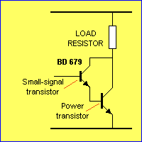
The BD 679 Darlington transistor is two transistors in one package, connected as shown in the diagram above. The upper transistor is a small-signal transistor and has its collector and base leads coming out of the package. The lower transistor has its collector and emitter leads coming out of the package. Obviously the collector lead is common to both transistors. 
When a voltage is applied to the base of this Darlington device, a current, flows into the base and turns the top transistor ON. Delivering current into the base is exactly the same as lifting the base a small amount with your finger. You don't need very much effort. The base is very easy to lift. This small effort is amplified by the transistor to the emitter and it lifts the emitter with the strength of about 100 times the effort you provided.
This "pulling-up" effect is now transferred to the base of the power transistor and it is equivalent to raising the base with 100 times more force than you exerted on the external base. 
The power transistor inside the device PULLS DOWN very strongly on the bottom of the LOAD RESISTOR and this allows a higher voltage to appear across the LOAD. The result is the load is activated. 
That's it. You lift the base UP very gently and the Darlington transistor pulls DOWN very strongly on the load resistor.

INSIDE THE BD 679


Inside the case of the BD 679 there are two transistors formed on a single silicon substrate, plus two resistors and a protection diode.
These components are connected together to form a "circuit" and it is important to know of their existence so that you can use the transistor correctly and understand the effect these components will have when the transistor is placed in a project.
For instance, the 10k resistor on the base will have an effect on the current required by the base to turn the transistor on. Normally, 1uA on the base of a Darlington would turn the transistor on but in our case the 10k base resistor lowers the input impedance (resistance) of the base considerably so that about 1mA is required. In fact, most of the current delivered into the base is lost in the biasing network. That's why we had trouble with one of our projects. 
Normally the transistor is used in a high current section of a circuit and these small losses are not significant.

RESISTANCE ANALOGY
Now for the resistance analogy. When no current flows into the base of the transistor, the resistance between the collector and emitter leads is very high. When you allow a small current to enter the base, the resistance between collector and emitter is reduced.
If you allow more current to pass into the base, the resistance between collector and emitter becomes even lower. For example, when no current flows into the base, the collector-emitter resistance may be 10Meg ohms or more.
For a small current into the base, the collector-emitter resistance may be 10k. When more current flows into the base, the collector-emitter resistance may be 100 ohms or as low as a few ohms.
If we have a resistor - called the LOAD RESISTOR - connect to the collector, we create a circuit similar to two resistors in SERIES and current will flow through the load resistor and transistor according to ohms law. As the resistance of the transistor decreases, the current through the pair increases.
There is nothing special about this, it is simple ohms law, as the transistor turns on harder, the current through the load resistor (and the transistor) increases.
If the resistance of the transistor decreases to a few ohms, you can see the current through the load will be a maximum and the device will be activated. 

CONVENTIONAL CURRENT APPROACH
The conventional current approach is the concept that current flows out the positive terminal of a battery and into the negative terminal.
In our case, when a small current flows into the base of the Darlington transistor, the collector-emitter circuit allows a larger current to flow.
When more current is allowed to flow into the base, the transistor will allow a greater current to flow in the collector-emitter circuit.
Since a load resistor is connected to the collector, this collector-emitter current will also flow in the load.

THE ELECTRON APPROACH
The electron approach basically says that electron flow occurs in the opposite direction to conventional current flow. In other words, electrons flow out the base to the positive rail and others flow in the emitter-collector circuit from the negative rail to the positive rail. The electron approach is  necessary if you want to describe the actual operation of transistor itself.

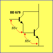
THE VOLTAGE APPROACH
One final way of looking at the operation of the circuit is the VOLTAGE approach.
The transistor does not turn on until a voltage of 0.65v + 0.65v  = 1.3v is supplied to the base lead. 
This voltage allows a small current to flow into the base and the voltage on the collector falls from rail voltage to slightly less than rail voltage. This puts a small voltage across the load and a small current flows in the load. 
As the voltage on the base is increase a few more millivolts, more current is able to flow into the base and the transistor multiplies this flow about 2,500 times and the increased current is allowed to flow in the collector-emitter circuit. 
Increasing the voltage on the base a few more millivolts will allow more current to flow into the base (in the order of milliamps) and very soon the maximum current will flow via the collector-emitter. 
If the load is a relay or globe, the device will be activated. 
You really need to combine all the concepts we have described to see how the transistor works.
Once you can see how the collector and emitter leads "squeeze" together or reduce in resistance, to deliver a current to the load, you will be able to see how the transistor works.

As more current is delivered to the load, this will introduce another feature you need to understand. It's called . . .

TRANSISTOR DISSIPATION
All the current through the load must flow through the transistor - this is obvious as the two are connected in series, and when current flows, heat is produced.
Unfortunately, transistors don't like to get hot and so the heating effect must be kept to a minimum.
When the transistor is off (no base voltage applied) no current flows and thus the heating effect is zero. This is obvious. 
This is one of the states of a transistor and is called "cut-off" or simply "off."
As the transistor gets turned on, more current flows and the heating effect increases.
Do you think this increase will be a maximum when the transistor is fully turned on?
No! Amazingly, the heating effect increases until half rail voltage appears on the collector and starts to reduce until it becomes nearly zero when the transistor is fully turned on. This state is called "saturation" or "bottoming."
This is a very important feature in electronics and means there are two states when the transistor is dissipating the minimum energy (heat) - the two states are: "bottoming" and "cut-off."
When a transistor is used in digital mode, it switches from one state (say cut-off) to the other (saturation) very quickly and very little heat is generated (lost) in the transistor.
But when a transistor is used in an audio application, it moves very slowly between one state and the other and a lot of heat is generated.
This heat must be passed to a heat-sink as quickly as possible to prevent the transistor heating up and self-destructing.
Self destruction may be final or partial and may produce loss of gain, an open circuit or a "short-circuit." Most often a transistor goes short-circuit.

BD 679 RATINGS 

MAXIMUM RATINGS: 
Collector-emitter voltage VCEO = 80v. The maximum voltage between collector and emitter when the transistor is NOT conducting.
Collector-base voltage VCBO = 80v
Collector current IC = 4amp. Maximum continuous collector current.
Collector peak current (t = less than 1mS) = 7 amp.
Base current IB = 100mA. The maximum current that can be fed into the base of the BD 679 without damaging the transistor. It is not the current required to turn it on fully - much less is required to turn it on fully.
Junction temperature Tj = 150°C
Total power dissipation 40 watts. This is the maximum wattage that can be dissipated by the transistor when it is adequately heat-sinked.
Minimum forward current gain (hFE @1.5amp) = 750
Typical forward current gain (hFE @1.5amp) = 2500
Maximum forward current gain (hFE @1.5amp) = 3500

GETTING MORE TECHNICAL 
Let's get a little more technical. One of the problems with the BD 679 is the minimum voltage between the collector-emitter terminals, when the transistor is fully turned on. This minimum voltage is about 2-3v, where as a normal transistor can go as low as .3v. For a MOSFET, the voltage can be .02v or lower.
Ideally, this voltage should be as low as possible as it determines the heat lost in the transistor when it is fully turned on. For instance, if a BD 679 is passing 4 amps in its saturated mode, the heat lost will be 2 x 4 = 8watts, or in the worst case, 3 x 4 = 12 watts.
For a MOSFET, the heat loss will be less than 0.08 watts.

WHY?
Why is the minimum collector-emitter voltage of a Darlinglon = 2.5v?
To see why, we need to see the diagram of the transistor as shown in the figure below:


The small-signal part of the Darlington is riding on top of the power transistor. As the collector of the power transistor falls during turn-on conditions, it pulls the collector of the small-signal transistor down with it and robs it of collector-emitter voltage.
This reduces the gain of the small-signal transistor and the collector-emitter current is also reduced so the power transistor will not be able to turn on as hard. This means the voltage on the collector will not fall below 2.5 volts as this leaves only about 2.5v - .65v = 1.85v, for the collector-emitter voltage of the small signal transistor.
This is just enough to give the transistor a collector voltage so that it can provide some gain to drive the power transistor.
This is one of the limitations of a Darlington transistor.

BASE VOLTAGE
Another characteristic of a Darlington transistor is the base voltage. It needs a voltage of 1.3v for the transistor to begin to turn on.
This compares with .65v for a normal transistor.
Darlington transistors consist of two transistors in a staircase arrangement and the base voltage is .65v + .65v = 1.3v. See diagram below:

 
The two base-emitter voltages combine to produce 1.3v to turn the Darlington transistor ON.
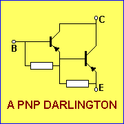

PNP DARLINGTON 
By combining two PNP transistors, a PNP Darlington transistor can be created. This is shown below. Matched pairs of PNP and NPN Darlington transistors can also be obtained so that a push-pull output can be created.
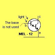

PHOTO DARLINGTON
Other Darlington devices can also be created. A photo-Darlington transistor is available under the part number MEL-12. This is a very sensitive device for detecting light and can be used for many applications such as photo-electric beams, light detection etc. The structure of the MEL-12 is shown below:

MEL-12 Photo Darlington Transistor

By building and experimenting with some of the projects we have described in this e-magazine you will get greater understanding of how a transistor works and how hot it can get before being damaged. To give an example, some of the first colour TV sets had the chrominance output transistors running so hot you could boil water on them. The latest sets use tiny plastic transistors and they run completely cold!  It's all in the way the circuit is designed. Circuits should always be designed so that everything runs cold. That way, things last forever.

INSIDE DARLINGTON TRANSISTORS 
The transistors inside the Darlington package can be arranged in a number of different ways. Apart from the NPN and PNP devices, some have resistors in the package while others have no resistors. Some have a reverse protection diode between the collector and emitter terminals and others have protection diodes on the base. Below is a selection of the circuits inside Darlington packages.
The base resistors are designed to prevent the transistor "turning on" due to natural leakage through the small signal transistor.
These circuits show that Darlington transistors are not all the same and cannot always be replaced with a different type. The different value of base resistor will mean different base currents will be required and you should always replace a device with the same type.


Freddy Vallenilla, CAF

viernes, 23 de julio de 2010

Mini Twin Transistor Shrinks VCO Designs


For shrinking VCO designs, the UPA828TD twin transistor combines two closely matched silicon NPN chips in a six-pin, leadless RoHS-compliant package measuring 1.2 mm x 1 mm x 0.5 mm. The device enables the combination of oscillator and buffer amplifier functions in one package. Typical specifications at 1V, 3 mA, and 2 GHz include a noise figure of 1.3 dB, an insertion power gain of 7.5 dB, and an operating frequency to 9 GHz. Each transistor is independently mounted, therefore the device is configurable for either cascode or dual transistor operation. Price is $0.06 each/10,000. 


Master The Fundamentals Of Your Gallium-Nitride Power Transistors


The basic design requirements for power semiconductors are efficiency, reliability, controllability, and cost-effectiveness. High-frequency capability adds further value in system size and transient response in regulators and fidelity in class D amplifiers. Without efficiency and reliability, a new device structure would have no chance of economic viability.

Many new structures and materials have been considered. Also, recent breakthroughs by EPC in processing gallium nitride (GaN) have produced enhancement-mode devices with high conductivity and hyper-fast switching, with a silicon-like cost structure and fundamental operating mechanism.

STRUCTURE
A device's cost effectiveness starts by leveraging existing production infrastructure. EPC's process begins with inexpensive silicon wafers. A thin layer of aluminum nitride (AlN) is grown on the silicon to isolate the device structure from the substrate. The isolation layer for 200 V and below devices is 300 V. On top of this, a thick layer of resistive GaN is grown. This provides a foundation on which to build the GaN transistor.

An electron-generating material is applied to the GaN. This layer creates a quantum strain field with an abundance of free electrons. Further processing forms a depletion region under the gate. To enhance the transistor, a positive voltage is applied to the gate in the same manner as turning on an n-channel, enhancement-mode power MOSFET (Fig. 1). This structure is repeated many times to form a power device. The end result is an elegant, cost-effective solution for power switching.


OPERATION
EPC's GaN transistors behave very similarly to silicon power MOSFETs. A positive bias on the gate relative to the source causes a field effect that attracts electrons that complete a bidirectional channel between the drain and the source. Since the electrons are pooled, as opposed to being loosely trapped in a lattice, the resistance of this channel is quite low. When the bias is removed from the gate, the electrons under it are dispersed into the GaN, recreating the depletion region, enabling it to block voltage.

To obtain a higher-voltage device, the distance between the drain and gate is increased. As the resistivity of our GaN electron pool is very low, the impact on RDS(on) (on resistance) by increasing the blocking voltage capability is much lower with GaN transistors compared to silicon. Figure 2 shows the theoretical resistance times die area limits of GaN and silicon versus voltage. EPC's first generation of devices is shown as well.


After 30 years of silicon MOSFET development, silicon is near its theoretical limit and progress has slowed to where small gains require significant development resources. GaN is young in its life cycle and will see significant improvement in the years to come.

GATE THRESHOLD
The threshold of GaN transistors is lower than that of silicon MOSFETs. This is possible because of the almost flat relationship between threshold and temperature along with the very low gate-to-drain capacitance (CGD). Figure 3 shows the transfer characteristics curve for the EPC1001, 100-V, 5.6-mΩ transistor. The negative relationship between current and temperature provides good sharing in the linear region. Because the device starts to conduct significant current at 1.6 V, a low impedance path is required from gate to source when the device needs to be held off during dV/dt.


RESISTANCE
RDS(on) versus gate-to-source voltage (VGS) curves are similar to MOSFETs. EPC's first-generation GaN transistors are designed to operate with 5-V drive. Figure 4 shows the set of curves for the EPC1001. The curve shows that RDS(on) continues to decrease as the absolute maximum gate voltage is approached.


As there is negligible gate drive loss penalty, GaN transistors should be driven with 5 V. The temperature coefficient of RDS(on) of the GaN transistor is positive. The magnitude is significantly less than MOSFETs. The 125°C point is 1.45 times the 25°C point for the EPC1001, compared to 1.7 for silicon. This advantage increases with increasing voltage.

CAPACITANCE
The lateral structure of the GaN transistor makes it a very low-charge device as well. It can switch hundreds of volts in nanoseconds, giving it multiple-megahertz capability. This will lead to smaller power converters and higher-fidelity class D amplifiers. Most important in switching is CGD. The EPC GaN FET's extremely low CGD leads to very rapid voltage switching. Gate-to-source capacitance (CGS) is large compared to CGD, giving GaN transistors excellent dV/dt immunity.

CGS is small when compared with silicon MOSFETs, giving them very short delay times as well as excellent controllability in low-duty-cycle applications. A 48- to 1-V buck regulator has been demonstrated at 1 MHz using 100-V GaN transistors from EPC. Drain-to-source capacitance (CDS) is also small versus silicon. Capacitance curves for GaN are similar to those for silicon except that with a similar resistance, its capacitance is significantly lower.

SERIES GATE RESISTANCE AND LEAKAGE
Series gate resistance (RG) limits how quickly the capacitance of a FET can be charged or discharged. Silicon MOSFETs are limited to using polysilicon or silicide where GaN transistors use metal gates. The metal gates enable GaN to have gate resistances of a couple tenths of an ohm. This low gate resistance also helps with dV/dt immunity. For isolating the gate, oxide growth is not an option with GaN. The gate leakage current of GaN transistors is higher than that of silicon MOSFETs. Gate leakage on the order of 1 mA should be expected.

FIGURE OF MERIT
Total gate charge (QG) is the integral of CGS plus CGD over voltage. A common figure of merit that accounts for both on-state and switching performance is (RDS(on) x QG). Figure 5 offers figures of merit for GaN transistors versus best-in-class silicon MOSFETs for 100-V devices. The RxQ figure of merit advantage increases as voltage increases.


BODY DIODE
As seen from Figure 1, EPC's GaN transistor structure is a purely lateral device, absent the parasitic bipolar junction common to silicon MOSFETs. As such, reverse bias or "diode" operation has a different mechanism but similar function. With zero bias gate to source, there is an absence of electrons under the gate region. As current is forced from source to drain, drain voltage decreases. A positive bias on the gate is created relative to the drift region, injecting electrons under the gate.

Once the gate threshold is reached, there will be sufficient electrons to form a conductive channel. The benefit to this mechanism is that no minority carriers are involved in conduction, and therefore no reverse recovery losses. While reverse recovery charge (QRR) is zero, output capacitance (COSS) has to be charged and discharged with every switching cycle.

For devices of similar RDS(on), GaN transistors have significantly lower COSS than silicon MOSFETs. As it takes threshold voltage to turn on the GaN transistor in the reverse direction, the forward voltage of the "diode" is higher than the silicon transistor. Therefore, care should be taken to minimize diode conduction.

PACKAGING
EPC's GaN transistors are insulated from the substrate. This allows monolithic fabrication of multiple transistors in any configuration in addition to efficient, common heatsinking without the need for an insulating interface. It also forces the current for both drain and source to be collected on one side of the die.

To keep the resistance low in the metal layers that collect the current, these paths must be kept short. To accomplish this, wafer level line grid arrays are used where drain and source lines are alternated. Standard line pitches are 0.4 mm and 0.6 mm. Figure 6 shows the EPC1010, a 200-V, 25-mΩ transistor. Underfill can be used where this does not allow compliance with safety agency creepage distance requirements.


APPLICATIONS AND VALUE
EPC brings the enhancement mode to GaN. This allows immediate realization of the disruptive gains in efficient high-frequency and low-duty-cycle power conversion. Other "exotic" technologies are either cost-prohibitive or use depletion mode. Depletion-mode devices lose control when there is no power. They also require new development in control ICs.

GaN transistors will yield a leap in class D audio technology by enabling efficient switching at frequencies above the AM band. Fidelity will approach class A and class AB systems without all of the size and weight limitations of linear amplifiers.

In information processing and storage systems, the whole power architecture can be reevaluated to take advantage of the switching capabilities. As output voltage increases for ac-dc converters, efficiency goes up. As bus voltage increases, transmission efficiency goes up. As frequency increases, size goes down.

EPC GaN enables the last stage, which permits the first two while increasing ac-dc efficiency when used as their synchronous rectifiers. They also allow for intermediate-stage converters to be removed for single-step conversion, saving the size and cost of the intermediate stage converter.


Freddy Vallenilla Roa.    CAF

Military Systems Bolstered By Building-Block Breakthroughs


Technological advances lead to tactical advantages. That's why investments in electronic technology for military applications traditionally run high. Yet those investments can often yield useful breakthroughs as well as dramatic improvements in existing technologies.

Military systems such as electronic warfare (EW), signal intelligence (SIGINT), and radar systems receive the most funding. Still, electronic building blocks such as amplifiers, display screens, software, and transistors enable those large systems and, hopefully, provide that tactical edge.

One of the most basic electronic building blocks is the transistor. Military system designers have long sought more power from a single device to achieve higher power densities in radar and EW transmitters for a given size. Two of the more significant developments in silicon transistor technology come from companies at the extremes of the supply curve: Freescale Semiconductor and HVVi Semiconductors. The former applies a traditional lateral silicon device architecture, while the latter employs a unique vertical configuration in its novel silicon transistors.

A CLOSER LOOK 
Freescale is well established for its laterally diffused metal-oxide-semiconductor (LDMOS) devices, especially for cellular basestations and other commercial comms systems. By extending its LDMOS process capabilities to 50-V transistor fabrication, it developed its model MRF6V14300H transistor for pulsed military systems, including radar and avionics systems (Fig. 1).


The Si LDMOS transistor is one of the first fruits of Freescale's sixth-generation Very High Voltage (VHV6) process. VHV6 is an evolution of the LDMOS process used to manufacture +28-V dc parts for commercial broadcast, communications, industrial, and medical applications, along with some military systems.

By operating at the higher bias voltage while maintaining good thermal dissipation, the MRF6V14300H can deliver 330-W peak output power with 17-dB power gain from 1200 to 1400 MHz. The output power is based on pulsed input signals with 300-µs pulse width with 12% duty cycle. Under those conditions, the transistor achieves 60% drain efficiency.

Taking a more unconventional approach, HVVi uses a vertical transistor architecture to obtain higher power levels at high frequencies, but also relies on a high supply voltage of +48 V dc. The company's patented high-voltage vertical field-effect-transistor (HVVFET) technology employs the transistor's foundation or substrate as the device drain.
The transistor depletes vertically into the substrate as the supply voltage is fed to the drain. It approaches planar breakdown in the vertical drain region, standing off maximum voltage with minimum on resistance. The technology forms the basis for the company's first three products, designed for high-power pulsed applications at L-band frequencies— Identify Friend or Foe (IFF), TCAS, TACAN, and Mode-S radar systems.

The lower-frequency PVV1011-300 HVVFET transistor is designed for 300-W pulsed output power from 1030 to 1090 MHz. It achieves that output level with 15-dB power gain and 48% drain efficiency when operating with 50-µs pulse-width input signals for a 1-ms pulse period.

The PVV1214-25 and PVV1214-100 HVVFETs provide higher frequency. The former delivers a 25-W output level from 1200 to 1400 MHz. The latter is rated for 100-W output power from 1200 to 1400 MHz. Both are characterized with 200-µs pulse-width input signals at a 10% pulse duty cycle.

Building on the HVVFET technology, HVVi has added a trio of transistors for airborne distance-measuring-equipment (DME) systems in the 1025- to 1150-MHz range. The HVV1012-060, HVV1012-100, and HVV1012-250 are designed for use with pulsed L-band signals. All three have been characterized with a +48-V dc supply and with 10-µs pulse-width signals at 1% duty cycle.

In spite of the novel architecture, these L-band power transistors are based on conventional silicon substrate materials, typically relying on multiple transistor cells in a push-pull configuration to achieve high output-power levels. Some transistor suppliers, such as Microsemi, have sought out more exotic device materials for higher transistor power, including silicon carbide (SiC) with its outstanding thermal properties, to dissipate the heat generated by the active device cells.

Microsemi's 0150SC-1250M and 0405SC-1000M RF power transistors are SiC-based static-induction transistors (SITs), single-ended designs with very simple impedance-matching requirements compared to typical silicon bipolar or LDMOS transistors. The Class AB transistors are about half the size of equivalent-power LDMOS or bipolar transistors.

The 0150SC-1250M typically provides 1400-W pulsed output power in the very high-frequency (VHF) band from 150 to 160 MHz. The 0405SC-1000M typically delivers 1100-W pulsed output power in the ultra-high-frequency (UHF) band from 406 to 450 MHz.

The SiC transistors are housed in single- ended flange-mount power packages, assembled with 100% gold metallization and gold wire bonds in hermetic packages for the highest reliability in hostile environments. They are ideal for solid-state power amplifiers for VHF weather radar and long-range tracking radar systems.

GENERATING SIGNALS 
Several oscillator/synthesizer products represented significant advances in signal-generation technology for military electronics systems. The VMEM5Q military clock oscillator from Vectron International builds on microelectromechanical- systems (MEMS) technology to provide the performance needed in the high-shock and high-vibration environments of military systems (Fig. 2). The clock oscillators, which can be specified with CMOS-compatible outputs at frequencies from 1 to 130 MHz, suit a wide range of military electronics applications, including smart munitions, missiles, and projectile electronics.


The rugged VMEM5Q oscillators withstand shock levels to 100,000 g. Qualification testing of a 125-MHz unit showed no degradation in performance at the maximum capabilities of the shock/ vibration test set, 30,000 g in each axis. They integrate PureSilicon Resonator MEMS resonators from Discera and feature CMOS-level output signals with typical rise/fall time of 5 ns with typical period jitter of only 7 ps.

For enhanced stability, the VMEM5Q oscillators include temperature compensation. They come in RoHS-compliant (Restrictions on Hazardous Substances) 5- by 3.2-mm quad flat no-lead (QFN) surface-mount packages and undergo extensive qualifications testing, including to MIL-PRF-55310 requirements.

Generating signals with a greater level of integration, the WaveCor SLO 2.0 source from the Microwave Systems division of ITT Corp. offers a frequency range of 50 MHz to 20.48 GHz based on direct-digital synthesis (DDS). With this technology, digital codes are converted to analog waveforms via digital-to-analog converters (DACs) and then upconverted in frequency, filtered, and amplified to reach a final required output range.

The WaveCor SLO 2.0 packs all of these functions into 6.00 by 6.00 by 2.75 in., weighing less than 5 lb. The compact DDS source tunes across that wide frequency range with 1-kHz resolution. Suitable for EW, radar, SIGINT, and automatic-test-equipment (ATE) systems, the device provides +14-dBm output power with ±1-dB flatness. It achieves low phase noise of -126 dBc/Hz measured at an offset of 10 kHz from a 10-GHz carrier signal.

DSP technology for military systems is also found within digital RF memory (DRFM), which captures continuouswave (CW) and pulsed threat signals for analysis. Essential components in many electronic-countermeasures (ECM) systems, DRFMs typically include a highspeed analog-to-digital converter (ADC) to transform analog inputs into digital code and a high-speed DAC to make the conversion back to analog signals.

A 10-bit DRFM from KOR Electronics is an integral part of several electronic- control module systems, available with as much as 1-GHz instantaneous capture bandwidth. Its high-resolution digitizing function is supported by a 12-bit DAC at the output port for high signal resolution and linearity.

Once a system captures signals, they still must be processed and displayed into meaningful results. UniPixel has made impressive improvements in color displays through its Time Multiplexed Optical Shutter (TMOS) technology. With TMOS, a single color source produces extremely short bursts of color, emitted so quickly that the eye combines the bursts as one color. The technique, known as "spatial additive color," uses different durations of blue, red, and green to create a variety of shades and hues.

Compared to plasma or LCD color screens, UniPixel displays require few layers, making them relatively less expensive to manufacture than conventional displays and with potentially greater reliability because of their simplicity. Prototype displays based on the technology have employed thin-film-transistor (TFT) structures and required only 12-V operating voltage with performance of 150 frames/second or better.

Military training has long depended on simulation software and hardware that depicts images in two dimensions, not drastically different than many video games. But two companies, EffectiveUI and Intelligence Gaming, intend to transform military simulations into realistic, 3D training exercises.

With the firms' RealityV video technology, users wear a head-mounted display and enter a lifelike, 360° video and sound simulated scenario that provides realistic simulation and training. The display gives a trainee realistic renditions of live action scenarios, as well as a taste of hostile situations. RealityV collects specific psychometric data during an exercise to determine a "player's" ability to handle new challenges and changing situations.

When it comes time to provide content for a military simulation, the Hurricane surveillance camera from Electrophysics Corp. can capture images during day or night. It combines a charge-coupleddevice (CCD) camera for daytime viewing with thermal imaging electronics for night-vision capabilities.

During the day, it provides about 630,000-pixel resolution in NTSC format and 740,000-pixel resolution in PAL format. At night, it can detect human signatures at distances of 2 km or more. It includes a vehicle mount and is tested to MIL-STD-810E requirements.


Freddy Vallenilla Roa.    CAF