Mostrando entradas con la etiqueta II 2010-1 CAF Freddy Vallenilla. Mostrar todas las entradas

domingo, 27 de junio de 2010

Common Source Amplifier with Source Degeneration.


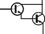
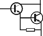
The small-signal amplification performance of the CS amplifier discussed in the previous lecture can be improved by including a series resistance in the source circuit. (This is very similar – if not identical – to the effect of adding emitter degeneration to the BJT CE amplifier.) This so-called CS amplifier with source degeneration circuit is shown in


We have a choice of small-signal models to use for the MOSFET. A T model will simplify the analysis, on one hand, by allowing us to incorporate the effects of RS by simply adding this value to 1/gm in the small-signal model, if we ignore ro. This small-signal circuit is shown in


On the other hand, using the T model makes the analysis more difficult when ro is included. (The hybrid ð model is better at easily including the effects of ro.) However, ro in the MOSFET amplifier is large so we can reasonably ignore its effects for now in the expectation of making the analysis more tractable. 

Small-Signal Amplifier Characteristics

We'll now calculate the following small-signal quantities for this MOSFET common source amplifier with source degeneration: Rin, Av, Gv, Gi, and Rout. 

• Input resistance, Rin. Referring to the small-signal equivalent circuit above in with I g=0 then

Rin = Rg

• Partial small-signal voltage gain, Av. We see at the output side of the small-signal circuit in 

V0= - gmVgs(RD||RL)

which is the same result (ignoring ro) as we found for the CS amplifier without source generation. At the gate, however, we find through voltage division that


This is a different result than for the CS amplifier in that vgs is only a fraction of vi here, whereas vgs =Vi without RS. Substituting (3) into (2), gives the partial small-signal AC voltage gain to be


• Overall small-signal voltage gain, Gv. As we did in the previous lecture, we can derive an expression for Gv in terms of Av. By definition, 


Applying voltage division at the input of the small-signal equivalent circuit in Fig. 4.44(b),


Substituting (6) into (5) we the overall small-signal AC voltage gain for this CS amplifier with source degeneration to be


• Overall small-signal current gain, Gi. Using current division at the output in the small-signal model above in


while at the input, 


Substituting (9) into (8) we find that the overall small-signal AC current gain is


• Output resistance, Rout. From the small-signal circuit in with vsig =0 then i must be zero leading to

Rout= RRD 

Discussion

Adding RS has a number of effects on the CS amplifier. (Notice, though, that it doesn't affect the input and output resistances.) First, observe from (3) 


that we can employ RS as a tool to lower vgs relative to vi and lessen the effects of nonlinear distortion. This RS also has the effect of lowering the small-signal voltage gain, which we can directly see from (7). A major benefit, though, of using RS is that the small-signal voltage (and current) gain can be made much less dependent on the MOSFET device characteristics. (We saw a similar effect in the CE BJT amplifier with emitter degeneration.) We can see this here for the MOSFET CS amplifier using (7)


The key factor in this expression is the second one. In the case that gm RS >> 1 then


which is no longer dependent on gm. Conversely, without RS in the circuit ( Rs =0 ), we see from (7) that Gva gm . and is directly dependent on the physical properties of the transistor (and the biasing) because


in the case of an NMOS device. The "price" we pay for this desirable behavior in (12) – where Gv is not dependent on gm – is a reduced value for Gv. This Gv is largest when Rs =0 , as can be seen from (7). 

Example N32.1 (based on text exercises 4.32 and 4.33). Compute the small-signal voltage gain for the circuit below with Rs =0 , kn' W/ L' =1 mA/V2 and Vt = 1.5 V. For a 0.4-Vpp sinusoidal input voltage, what is the amplitude of the output signal? 


For the DC analysis, we see that VG =0 and ID= IS = 0.5 mA. (Why is VG = 0?) Consequently, 

VD =10 - RDID =10 -14 K •5m = 3V Assuming MOSFET operation in the saturation mode

Assuming MOSFET operation in the saturation mode


such that


or

VGS-1.5=+1 VGS=2.5 or 0.5V

Therefore 

Vs = - 2.5 V

for operation in the saturation mode. For the AC analysis, from (13) g<m= 10=(2.5-1.5)=1 mS Using this result in (7) with Rs =0 gives


For an input sinusoid with 0.4-Vpp amplitude, then

V0Gv . Vsig=6.85.0.4 V pp = 2.74 Vpp

Will the MOSFET remain in the saturation mode for the entire cycle of this output voltage? For operation in the saturation mode, vDG= vD >Vt = 1.5 V. On the negative swing of the output voltage, 


which is greater than Vt, so the MOSFET will not leave the saturation mode on the negative swings of the output voltage. On the positive swings, 


which is less than VDD = 10 V so the MOSFET will not cutoff and leave the saturation mode. (Interestingly, the MOSFET does leave the saturation mode on the negative swings for 15 RD= RL = 15 k beta, as used in the text exercises 4.32 and 4.33.) Lastly, imagine that for some reason the input voltage is increased by a factor of 3 (to 1.2 Vpp). What value of RS can be used to keep the output voltage unchanged? 

Lastly, imagine that for some reason the input voltage is increased by a factor of 3 (to 1.2 Vpp). What value of RS can be used to keep the output voltage unchanged? From (7), we can choose RS so that the so-called feedback factor 1+ gm Rs equals 3. The output voltage amplitude will then be unchanged with this increased input voltage.Hence, for


With R s=2 k beta the new overall small-signal AC voltage gain is from (7) 


The overall small-signal voltage gain has gone down, but the amplitude of the output voltage has stayed the same since the input voltage amplitude was increased. 


Freddy R Vallenilla R
16.791.006
CAF

Power supply circuits


There are three major kinds of power supplies: unregulated (also called brute force), linear regulated, and switching. A fourth type of power supply circuit called theripple-regulated, is a hybrid between the "brute force" and "switching" designs, and merits a subsection to itself.

Unregulated

An unregulated power supply is the most rudimentary type, consisting of a transformer, rectifier, and low-pass filter. These power supplies typically exhibit a lot of ripple voltage (i.e. rapidly-varying instability) and other AC "noise" superimposed on the DC power. If the input voltage varies, the output voltage will vary by a proportional amount. The advantage of an unregulated supply is that it's cheap, simple, and efficient.

Linear regulated

A linear regulated supply is simply a "brute force" (unregulated) power supply followed by a transistor circuit operating in its "active," or "linear" mode, hence the namelinear regulator. (Obvious in retrospect, isn't it?) A typical linear regulator is designed to output a fixed voltage for a wide range of input voltages, and it simply drops any excess input voltage to allow a maximum output voltage to the load. This excess voltage drop results in significant power dissipation in the form of heat. If the input voltage gets too low, the transistor circuit will lose regulation, meaning that it will fail to keep the voltage steady. It can only drop excess voltage, not make up for a deficiency in voltage from the brute force section of the circuit. Therefore, you have to keep the input voltage at least 1 to 3 volts higher than the desired output, depending on the regulator type. This means the power equivalent of at least 1 to 3 volts multiplied by the full load current will be dissipated by the regulator circuit, generating a lot of heat. This makes linear regulated power supplies rather inefficient. Also, to get rid of all that heat they have to use large heat sinks which makes them large, heavy, and expensive.

Switching

A switching regulated power supply ("switcher") is an effort to realize the advantages of both brute force and linear regulated designs (small, efficient, and cheap, but also "clean," stable output voltage). Switching power supplies work on the principle of rectifying the incoming AC power line voltage into DC, re-converting it into high-frequency square-wave AC through transistors operated as on/off switches, stepping that AC voltage up or down by using a lightweight transformer, then rectifying the transformer's AC output into DC and filtering for final output. Voltage regulation is achieved by altering the "duty cycle" of the DC-to-AC inversion on the transformer's primary side. In addition to lighter weight because of a smaller transformer core, switchers have another tremendous advantage over the prior two designs: this type of power supply can be made so totally independent of the input voltage that it can work on any electric power system in the world; these are called "universal" power supplies.

The downside of switchers is that they are more complex, and due to their operation they tend to generate a lot of high-frequency AC "noise" on the power line. Most switchers also have significant ripple voltage on their outputs. With the cheaper types, this noise and ripple can be as bad as for an unregulated power supply; such low-end switchers aren't worthless, because they still provide a stable average output voltage, and there's the "universal" input capability.

Expensive switchers are ripple-free and have noise nearly as low as for some a linear types; these switchers tend to be as expensive as linear supplies. The reason to use an expensive switcher instead of a good linear is if you need universal power system compatibility or high efficiency. High efficiency, light weight, and small size are the reasons switching power supplies are almost univerally used for powering digital computer circuitry.

Ripple regulated

A ripple-regulated power supply is an alternative to the linear regulated design scheme: a "brute force" power supply (transformer, rectifier, filter) constitutes the "front end" of the circuit, but a transistor operated strictly in its on/off (saturation/cutoff) modes transfers DC power to a large capacitor as needed to maintain the output voltage between a high and a low setpoint. As in switchers, the transistor in a ripple regulator never passes current while in its "active," or "linear," mode for any substantial length of time, meaning that very little energy will be wasted in the form of heat. However, the biggest drawback to this regulation scheme is the necessary presence of some ripple voltage on the output, as the DC voltage varies between the two voltage control setpoints. Also, this ripple voltage varies in frequency depending on load current, which makes final filtering of the DC power more difficult.

Ripple regulator circuits tend to be quite a bit simpler than switcher circuitry, and they need not handle the high power line voltages that switcher transistors must handle, making them safer to work on.


Freddy R Vallenilla R
16.791.006
CAF


Transistor Darlington Pair


The Darlington Pair is a useful circuit configuration for many applications within electronic circuits. The Darlington transistor configuration provides a number of advantages that other forms of transistor circuit are not able to offer and as a result it is used in many areas of electronics design. The Darlington Pair also occasionally referred to as a super-alpha pair is renowned as a method for obtaining a very high level of current gain, using just two transistors. It is able to provide levels of gain that are not possible using single transistors on their own, but it may not be used in all circumstances because it does have a number of limitations.
The Darlington Pair may be used in the form of discrete components, but there are also very many integrated circuit versions often termed a Darlington transistor that may also be used. These Darlington transistor components may be obtained in a variety of forms including those for high power applications where current levels of many amps may be required.
The Darlington Pair has been in use for very many years. It was invented in 1953 by Sidney Darlington who was working at Bell Laboratories. He developed the idea of having two or three transistors in a single semiconductor chip, where the emitter of one transistor was connected directly to the base of the next, and all the transistors shared the same collector connection. In many ways the Darlington bore many of the hallmarks of the first integrated circuit patent, but it was too specific to the specific Darlington circuit itself to be considered as an integrated circuit.


Darlington pair basics

When using an emitter follower in a circuit, the level of current gain, and the input impedance of the circuit is limited by the current gain that can be achieved using a single transistor. The gain of the Darlington transistor pair is that gain of the two individual transistors multiplied together.


Current gaintotal     =     HFE1   x   HFE2


The basic Darlington transistor circuit is formed by taking the emitter of the input transistor and connecting it such that its emitter drives the base of the second and then connecting both collectors together. This circuit can be used as any single transistor would be in a variety of circuits, but particularly as an emitter follower.

Basic Darlington Pair transistor configuration


Basic Darlington Pair transistor configuration

In many respects a Darlington pair can be treated like a single transistor with a very high gain, and in these instances it is often shown on a circuit diagram as a single component.

Circuit symbol for a Darlington pair chip


Circuit symbol for a Darlington pair chip

While the Darlington can be viewed almost as a circuit block or component in its own right, it does have several differences between it and the basic transistor. For example it has a higher voltage difference between the overall base and emitter, i.e. from the base of the input transistor to the emitter of the output transistor.


VBE   =   VBE1   +   VBE2


This means that for a typical silicon device, the overall base emitter voltage required to turn the Darlington pair on is two times 0.7 volts, i.e. 1.4 volts.
A further point to note is that the saturation voltage of the Darlington configuration is about 0.7 volts. This is higher than that of a single transistor, where, for example a switching transistor may exhibit a saturation voltage of around 0.2 volts. The increased level of saturation voltage of the Darlington pair needs to be considered in some applications where high currents are passed because it may result in significant levels of power being dissipated in the device.
It is also necessary to be aware that the Darlington Pair is not as fast as a single transistor. This is because the first transistor cannot actively shut off the base current of the second transistor. In turn this makes the overall device or circuit configuration slow to reduce the current flow or switch off. To address this problem, the second transistor often has a resistor connected between the base and emitter. This resistor also helps prevent any leakage current from the input transistor from turning the output transistor on. This leakage current can be of the order of nano-amps for a small signal transistor or up to a few hundred micro-amps for a power transistor. The value of the base emitter resistor is chosen so that it does not sink a large proportion of the current intended to pass through the base of the output transistor, while not allowing the leakage current to develop a voltage equal to the turn on voltage of the output transistor to be developed. Typical values for the resistor may be a few hundred ohms for a power transistor Darlington or a few thousand ohms for a small signal version.

Darlington circuit including base resistor


Darlington circuit including base resistor

When using a Darlington pair configuration in a new electronics design, it is necessary to account for the fact that it has a greater phase shift at high frequencies than a single transistor. This can result in the overall circuit having a greater likelihood of becoming unstable if negative feedback is used in the circuit.
Often when making a Darlington pair, the output transistor is required to be able to handle high levels of current. High power transistors typically have lower levels of current gain than the small signal varieties. This means that often the input device in the Darlington pair or Darlington transistor is a small signal high gain variety, whereas the output transistor is a high power device with an inherently lower current gain.


Darlington pair advantages and disadvantages summary

While the Darlington pair offers many advantages they also have limitations. Accordingly when considering the use of the Darlington pair, it is necessary to weigh up both sides of the equation.


ADVANTAGES:DISTADVANTAGES:
  • Very high current gain
  • Very high input impedance for overall circuit
  • Darlington pairs are widely available in a single package or they can be made from two separate transistors
  • Convenient and easy circuit configuration to use
  • Slow switching speed
  • Limited bandwidth
  • Introduces a phase shift that can give rise to problems at certain frequencies in circuit using negative feedback
  • Higher overall base-emitter voltage = 2 x Vbe.
  • High saturation voltage (typically around 0.7 V) which can lead to high levels of power dissipation in some applications


Darlington pair applications

Darlington pairs find applications in many areas. Offering a very high level of current gain they can be used to good effect in many areas. However when using the Darlington pair, its limitations must also be considered. As a result, its use is limited to a number of areas where its limitations are not a major problem. Some typical areas where the Darlington is used include:
  • Audio power output stages:   Sometimes audio amplifier power output stages may require significant levels of current gain to enable them to drive low impedance speakers. The limited bandwidth and is unlikely to affect the frequency response over the frequency ranges being used.
  • Linear power regulators:   The Darlington circuit configuration is ideal for use in linear power regulators. There is a requirement for the circuit to be able to drive high current levels and in this respect high levels of current gain are required. It is necessary to consider the slow response on the suppression of spikes in the design.
  • Photo-Darlington:   Phototransistors are widely used in sensors. To improve the sensitivity of these devices, photodarlingtons are available. These offer considerably higher levels of sensitivity and as a result they are widely used.
  • General high power applications:   The high current gain capability of the Darlington transistor makes it ideal for controlling high current levels. As a result special Darlington transistor modules are available that are able to carry current levels of 100 amps and more. These Darlington transistor modules are often relatively large and employ screw terminals and are designed for mounting on large heat-sinks. Possible end applications for these devices may include inverter circuits, AC motor control, DC motor control circuits and emergency power supplies, etc..
  • LED and Display drivers:   Darlington transistor arrays contained within IC packages are widely used for driving loads from standard logic families. Here high levels of current gain are required, making the Darlington an ideal choice. Typical arrays are suitable for driving LEDs, displays, solenoids or other loads. Often these arrays have built in suppression diodes to prevent any reverse voltages (back EMFs) from any inductive loads from destroying them when the current is switched off.
These are only a few examples of where the Darlington pair configuration can be used. They can be used in many other areas where high current gain is needed.


Darlington pair summary

The Darlington pair transistor circuit configuration can be very useful in electronics circuit design. Although it has speed limitations, the Darlington Pair is nevertheless very useful in many areas where high levels of current gain are required, particularly for emitter follower style applications.
Although the Darlington pair is most usually referred to by this name, the older name - the super-alpha pair may still be used on some occasions. This name for the Darlington, was more widely used in the 1960s, and its has largely been superseded, although it may persist in some areas.

Freddy R Vallenilla R
16.791.006
CAF