Mostrando entradas con la etiqueta Reyes Vargas Jairo Alberto. Mostrar todas las entradas

lunes, 15 de febrero de 2010

Differential Amplifier


CIRCUIT
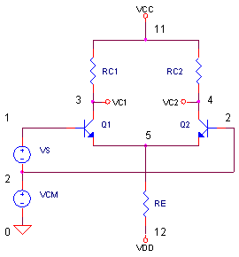
Look under the hood of most op amps, comparators or audio amplifiers, and you'll discover this powerful front-end circuit - the differential amplifier. A simple circuit able to amplify small signals applied between its two inputs, yet reject noise signals common to both inputs. This circuit has a unique topology: two inputs and two outputs. Although you can tap the signal from one output only, taking the difference between both outputs delivers twice the gain! And it improves Common-Mode Rejection (CMR), an essential function when the common-mode signal is a noise source or DC bias from a previous stage.

GAIN AND REJECTION
How does this amplifier amplify differential signals and reject common ones? The bias condition assumes equal voltages at VB1 and VB2, forcing the bias current IE (set by RE) to split equally between the transistors resulting in IC1 = IC2. With RC1 = RC2, equal voltages develop at VC1 and VC2. 
DIFFERENTIAL GAIN
Now suppose a differential signal is applied to the inputs. This will incrementally increase and decrease the base voltages to
VB1 + ΔV  and  VB2 - ΔV
Because Q1 conducts a little more and Q2 a little less, IE now splits unevenly creating
IC1 IC2
This, in turn, forces the voltage at VC1 to decrease and VC2 to increase. The result: a voltage change at each output due to a differential input.

COMMON-MODE REJECTION
Now suppose a common-mode input signal is applied. We incrementally increase both inputs to
VB1 + ΔV  and  VB2 + ΔV
Because the conduction level of neither transistors has changed (both bases and emitters moved by the same amount), the collector currents did not change.
IC1 = IC2  IE / 2.
Subsequently, the voltages at VC1 and VC2 remain the same! Therefore, the circuit has rejected a signal common to both inputs.
Well, the last statement is almost true. Actually, a change in emitter voltage had a small ill effect. It changed the bias current IE set by RE. And this directly impacted IC1 = IC2 IE / 2, slightly shifting the levels at VC1, VC2. As you can see the rejection is not perfect. However, it can still be effective at removing a large part of noise or a DC bias common to both inputs.

DIFFERENTIAL GAIN
How do we calculate the differential voltage gain? You can think of Q1 and Q2 as current sources controlled by their base voltages. RC1 and RC2 then convert the currents back into voltages. First, the small signal collector current
iC = gm ∙ vB
where the transconductance gm  (A / V) is set by the DC collector current 
gm = Ic / V
= Ic / 25 mV
 at room temperature. Then, RC transforms ic back to a voltage
vC = R∙ gm ∙ vB
Getting the input VS into the picture, notice it divides equally across each base-emitter junction, but with opposite polarities. Putting it all together you get a single-ended output for each transistor
vC1 = RC1 ∙ gm +VS / 2
vC2 = RC2 ∙ gm ∙ -VS / 2
Subtracting the two outputs gets you a differential output of
vC1 - vC2 = R∙ gm ∙ VS
What about the bias current? RE sets the bias at  Ie = (-0.6V - VDD) / RE = (-0.6 V - (-15 V)) / 7.2 k = 2 mA which divides equally between Q1 and Q2 giving 
Ic1 = Ic2 ≈ Ie / 2 ≈ 1 mA
Finally, we easily calculate gm = 1 mA / 25 mV = 0.04 A/V. The single-ended gain becomes
vC1 / VS = RC1 ∙ gm ∙ 1/2
              
= 1 k ∙ 0.04 ∙ 1/2
              = 20 V/V
 CIRCUIT INSIGHT   Run a simulation of BJT_DIFFAMP1.CIR. For VS = 10 mV peak, do you see about 200 mV peak at V(3)? Check out the signal at V(4). Is it equal and opposite to V(3)? To double the gain, remove traces V(3) and V(4) and plot the difference between the two outputs:
V(3)-V(4) or V(3,4).

 HANDS-ON DESIGN   How can you adjust the gain? Notice, that RE sets Ic, which determines gm, which directly sets the gain. So to decrease the gain by a factor of 2 or 3, for example, just increase RE by a factor of 2 or 3. Looking at the output equation, how else can you adjust gain? Try adjusting the values of RC1 and RC2 to vary the gain.

COMMON MODE REJECTION
 CIRCUIT INSIGHT   To see the CMR in action, zero the signal source by setting VS to 0MVPEAK. Then turn up VCM to something like 100MVPEAK. Run a new simulation. What happens at both
V(3) and V(4)? Notice the output voltages are very small! And to boot, they move in the same direction. This can work in our favor if we're able to take the difference between outputs, V(3,4). This
differential output further improves the CMR! Now, try mismatching the RCs by a percent or two and watch what happens at V(3,4).
In practice, how do you take the difference? Simply follow a differential amplifier with another differential amplifier. Or, like in op amp circuits, subtract the collector currents directly using additional transistors to mirror current from one collector to another. ( A future design topic to be sure.)


HOW MUCH DISTORTION?
 HANDS-ON DESIGN    How big can VS be before the output becomes distorted. Restore VS back to 10MVPEAK and set VCM to 0MVPEAK. Rerun the diff amp simulation and plot V(3,4). Okay, it looks pretty normal. Now, turn VS up to something like 20, 50 or 100 mV. What's happening to the natural beauty of the output sinewave?
Want a better view of the input / output transfer curve? You're not limited to plotting time on the X-axis. In fact, you can change it to a different variable. ( Most simulators let do this by clicking on the X-Axis or via a pull-down menu item.) Try plotting V(3,4) on the Y-Axis and V(1) on the X-Axis. How much of this input / output curve is actually a straight line?

THD
If you're interested, SPICE can calculate the Total Harmonic Distortion (THD). For example, including the statement
.FOUR 10KHZ V(3,4)
asks SPICE to calculate the percentage of higher harmonics to the 10 kHz fundamental sinewave in the waveform at V(3,4). If its all 10 kHz fundamental and no harmonics, you've got pure sinewave dancing at the output. However, as is typical in most amplifiers, the larger signal, the more distorted it gets.
Run a few simulations while increasing VS beyond 10 mV. Checkout the THD results appearing in the in the output text file, BJT_DIFFAMP1.OUT.

VOLTAGE-CONTROL AMPLIFIER
The differential amplifier makes a handy Voltage-Controlled Amplifier (VCA). All you need to do is vary the emitter bias current ( which of course varies the transistor's transconductance.) How? One way is to replace the -15 VDC supply with a voltage source that varies. For example, use a PWL statement to linearly ramp VDD slowly (say over 1000us ) from -5 V to -15 V. Does the output at V(3,4) increase over time? Remember to increase the total time for the transient analysis as needed.

LEVEL SHIFTING
The current-source nature of the transistor's output provides a big benefit. You can shift the output to different voltage levels. If the next stage needs a voltage biased around 25 V, for example, simply change VCC to a higher voltage. Although the output DC bias voltage will be higher, the gain should remain basically the same.
You can also shift the output to a negative rail! Just flip the entire circuit upside down and swap the NPN transistors for PNPs. Many op amps and audio amps shift the output to the negative rail, delivering the signal to the next stage, the Miller Integrator.

SPICE FILE
BJT_DIFFAMP1.CIR - BJT DIFFERENTIAL AMPLIFIER
* * SIGNAL SOURCE VS 1 2 AC 1 SIN(0 10MVPEAK 10KHZ) VCM 2 0 SIN(0 0MVPEAK 5KHZ) * * POWER SUPPLIES VCC 11 0 DC +15V VDD 12 0 DC -15V * Q1 3 1 5 Q2N2222 Q2 4 2 5 Q2N2222 RC1 11 3 1000 RC2 11 4 1000 RE 5 12 7.2K * * .model Q2N2222  NPN(Is=3.108f Xti=3 Eg=1.11 Vaf=131.5 Bf=217.5 Ne=1.541 +               Ise=190.7f Ikf=1.296 Xtb=1.5 Br=6.18 Nc=2 Isc=0 Ikr=0 Rc=1 +               Cjc=14.57p Vjc=.75 Mjc=.3333 Fc=.5 Cje=26.08p Vje=.75 +               Mje=.3333 Tr=51.35n Tf=451p Itf=.1 Vtf=10 Xtf=2 Rb=10) * * * CHECK DISTORTION WITH FOURIER SERIES ANALYSIS .FOUR 10KHZ V(3,4) * * ANALYSIS .TRAN  5US  200US .AC  DEC  5 1K 100MEG * * VIEW RESULTS .PRINT TRAN  V(3) .PRINT AC  V(3) .PROBE .END
Fuente: Link
Hecho Por:
Reyes Vargas Jairo Alberto

MIT Shows New Transistor Technology


MIT engineers have demonstrated a technology that could introduce an important new phase of the microelectronics revolution that has already brought us iPods, laptops and much more.
The work was presented at the recent IEEE International Electron Devices Meeting by Dae-Hyun Kim. Kim is a postdoctoral associate in the laboratory of Jesus del Alamo, an MIT professor of electrical engineering and computer science and member of MIT's Microsystems Technology Laboratories (MTL).
"Unless we do something very radical pretty soon, the microelectronics revolution that has enriched our lives in so many different ways might come to a screeching halt," said del Alamo.
The problem" Engineers estimate that within the next 10 to 15 years we will reach the limit, in terms of size and performance, of the silicon transistors key to the industry. "Each of us has several billion transistors working on our behalf every day in our phone, laptop, iPod, car, kitchen and more," del Alamo noted.
As a result, del Alamo's lab and others around the world are working on new materials and technologies that may be able to reach beyond the limits of silicon. "We are looking at new semiconductor materials for transistors that will continue to improve in performance, while devices get smaller and smaller," del Alamo said.
One such material del Alamo and his students at the MTL are investigating is a family of semiconductors known as III-V compound semiconductors. Unlike silicon, these are composite materials. A particularly hot prospect is indium gallium arsenide, or InGaAs, a material in which electrons travel many times faster than in silicon. As a result, it should be possible to make very small transistors that can switch and process information very quickly.
Del Alamo's group recently demonstrated this by fabricating InGaAs transistors that can carry 2.5 times more current than state-of-the-art silicon devices. More current is the key to faster operation. In addition, each InGaAs transistor is only 60 nanometers, or billionths of a meter, long. That's similar to the most advanced 65-nanometer silicon technology available in the world today.
"The 60-nanometer InGaAs quantum-well transistor demonstrated by Professor del Alamo's group shows some exciting results at low supply voltage (e.g. 0.5V) and is a very important research milestone," said Robert Chau, senior fellow and director of transistor research and nanotechnology at Intel, a sponsor of the work.
Del Alamo notes, however, that InGaAs transistor technology is still in its infancy. Some of the challenges include manufacturing transistors in large quantities, because InGaAs is more prone to breakage than silicon. But del Alamo expects prototype InGaAs microdevices at the required dimensions to be developed over the next two years and the technology to take off in a decade or so.
"With more work, this semiconductor technology could greatly surpass silicon and allow us to continue the microelectronics revolution for years to come," del Alamo said.
Fuente: Link
Hecho Por:
Reyes Vargas Jairo Alberto

New Transistor Mimics Synapse Functions


Talk of androids, advanced computer-based brain simulations and war robots is very exiting, but the development of artificial intelligence has been slightly stumped by a lack of transistors that work like our brains do. Until now.
Now, thanks to scientists in France, we have the NOMFET--the nanoparticle organic memory field-effect transistor. It's an organic-based device that uses pentacene and gold nanoparticles. The pentacene is a coating on the gold, which is embedded in the channel of a semiconducting transistor. This results in the transistor having the same type of switching/amplification behavior as a usual transistor with the benefits of a sort of "memory effect."
The upshot of this memory effect is that the NOMFET behaves in a similar way to the manner of an organic synapse as it transmits a signal between neurons--it can modify its reaction to incoming signals based on events that happened before, or on the nature of the signal it's dealing with at that moment. As a result it will allow for simplified chip-based simulations of a brain-type system, with far fewer semiconductor components than have been needed previously. 
This has repercussions for neuron-inspired artificial brain designs, which may now be more densely constructed. The technology of artificial brains may be significantly boosted as a result--which means we may see better machine vision hardware. And, of course, the artificial synapses may be used to boost the artificial intelligence of the sort of robots that get sci-fi fans all hot under the collar.
Fuente: Link
Hecho Por:
Reyes Vargas Jairo Alberto

The Cascode Amplifier


While the C-B (common-base) amplifier is known for wider bandwidth than the C-E (common-emitter) configuration, the low input impedance (10s of Ω) of C-B is a limitation for many applications. The solution is to precede the C-B stage by a low gain C-E stage which has moderately high input impedance (kΩs). See Figure below. The stages are in a cascode configuration, stacked in series, as opposed to cascaded for a standard amplifier chain. See “Capacitor coupled three stage common-emitter amplifier” Capacitor coupledfor a cascade example. The cascode amplifier configuration has both wide bandwidth and a moderately high input impedance.

The cascode amplifier is combined common-emitter and common-base. This is an AC circuit equivalent with batteries and capacitors replaced by short circuits.
The key to understanding the wide bandwidth of the cascode configuration is the Miller effect Miller effect. It is the multiplication of the bandwidth robbing collector-base capacitance by beta. This C-B capacitance is smaller than the E-B capacitance. Thus, one would think that the C-B capacitance would have little effect. However, in the C-E configuration, the collector output signal is out of phase with the input at the base. The collector signal capacitively coupled back opposes the base signal. Moreover, the collector feedback is beta times larger than the base signal. Thus, the small C-B capacitance appears beta times larger than its actual value. This capacitive gain reducing feedback increases with frequency, reducing the high frequency response of a C-E amplifier.
A common-base configuration is not subject to the Miller effect because the grounded base shields the collector signal from being fed back to the emitter input. Thus, a C-B amplifier has better high frequency response. To have a moderately high input impedance, the C-E stage is still desirable. The key is to reduce the gain (to about 1) of the C-E stage to reduce the Miller effect C-B feedback to 1·CCB. The total C-B feedback is the Miller capacitance 1·CCB plus the actual capacitance CCB for a total of 2·CCB. This is a considerable reduction from β·CCB.
The way to reduce the common-emitter gain is to reduce the load resistance. The gain of a C-E amplifier is approximately RC/RE. The internal emitter resistance REE at 1mA emitter current is 26Ω. For details on the 26Ω, see “Derivation of REE”, see REE. The collector load RC is the resistance of the emitter of the C-B stage loading the C-E stage, 26Ω again. CE gain amplifier gain is approximately RC/RE=26/26=1. We now have a moderately high input impedance C-E stage without suffering the Miller effect, but no dB voltage gain. The C-B stage provides a high voltage gain. Thus, the cascode has moderately high input impedance of the CE, good gain, and good bandwidth of the C-B.

SPICE: Cascode and common-emitter for comparison.
The SPICE version of both a cascode amplifier, and for comparison, a common-emitter amplifier is shown in Figure above. The netlist is in Table below. The AC source V3 drives both amplifiers via node 4. The bias resistors for this circuit are calculated in an example problem cascode.

SPICE waveforms. Note that Input is multiplied by 10 for visibility.

SPICE netlist for printing AC input and output voltages.

*SPICE circuit <03502.eps> from XCircuit v3.20 V1 19 0 10 Q1 13 15 0 q2n2222 Q2 3 2 A q2n2222 R1 19 13 4.7k V2 16 0 1.5 C1 4 15 10n R2 15 16 80k Q3 A 5 0 q2n2222 V3 4 6 SIN(0 0.1 1k)  ac 1 R3 1 2 80k R4 3 9 4.7k C2 2 0 10n C3 4 5 10n R5 5 6 80k V4 1 0 11.5 V5 9 0 20 V6 6 0 1.5 .model q2n2222 npn (is=19f bf=150 + vaf=100 ikf=0.18 ise=50p ne=2.5 br=7.5 + var=6.4 ikr=12m isc=8.7p nc=1.2 rb=50 + re=0.4 rc=0.3 cje=26p tf=0.5n + cjc=11p tr=7n xtb=1.5 kf=0.032f af=1) .tran 1u 5m .AC DEC 10 1k 100Meg .end 
The waveforms in Figure above show the operation of the cascode stage. The input signal is displayed multiplied by 10 so that it may be shown with the outputs. Note that both the Cascode, Common-emitter, and Va (intermediate point) outputs are inverted from the input. Both the Cascode and Common emitter have large amplitude outputs. The Va point has a DC level of about 10V, about half way between 20V and ground. The signal is larger than can be accounted for by a C-E gain of 1, It is three times larger than expected.

Cascode vs common-emitter banwidth.
Figure above shows the frequency response to both the cascode and common-emitter amplifiers. The SPICE statements responsible for the AC analysis, extracted from the listing:


V3 4 6 SIN(0 0.1 1k)  ac 1 .AC DEC 10 1k 100Meg 


Note the “ac 1” is necessary at the end of the V3 statement. The cascode has marginally better mid-band gain. However, we are primarily looking for the bandwidth measured at the -3dB points, down from the midband gain for each amplifier. This is shown by the vertical solid lines in Figure above. It is also possible to print the data of interest from nutmeg to the screen, the SPICE graphical viewer (command, first line):

nutmeg 6 -> print frequency db(vm(3)) db(vm(13))  Index   frequency     db(vm(3))  db(vm(13))  22      0.158MHz      47.54      45.41 33      1.995MHz      46.95      42.06 37      5.012MHz      44.63      36.17 
Index 22 gives the midband dB gain for Cascode vm(3)=47.5dB and Common-emitter vm(13)=45.4dB. Out of many printed lines, Index 33 was the closest to being 3dB down from 45.4dB at 42.0dB for the Common-emitter circuit. The corresponding Index 33 frequency is approximately 2Mhz, the common-emitter bandwidth. Index 37 vm(3)=44.6db is approximately 3db down from 47.5db. The corresponding Index37 frequency is 5Mhz, the cascode bandwidth. Thus, the cascode amplifier has a wider bandwidth. We are not concerned with the low frequency degradation of gain. It is due to the capacitors, which could be remedied with larger ones.
The 5MHz bandwith of our cascode example, while better than the common-emitter example, is not exemplary for an RF (radio frequency) amplifier. A pair of RF or microwave transistors with lower interelectrode capacitances should be used for higher bandwidth. Before the invention of the RF dual gate MOSFET, the BJT cascode amplifier could have been found in UHF (ultra high frequency) TV tuners.
  • REVIEW
  • cascode amplifier consists of a common-emitter stage loaded by the emitter of a common-base stage.
  • The heavily loaded C-E stage has a low gain of 1, overcoming the Miller effect
  • .
  • cascode amplifier has a high gain, moderately high input impedance, a high output impedance, and a high bandwidth.
Fuente: Link

Hecho Por:
Reyes Vargas Jairo Alberto

Transistor Darlington

En electrónica, el transistor Darlington es un dispositivo semiconductor que combina dos transistores bipolares en un tándem (a veces llamado par Darlington) en un único dispositivo.
La configuración (originalmente realizada con dos transistores separados) fue inventada por el ingeniero de los Laboratorios Bell Sidney Darlington. La idea de poner dos o tres transistores sobre un chip fue patentada por él, pero no la idea de poner un número arbitrario de transistores que originaría la idea moderna de circuito integrado.

Diagrama de la Configuracion Darlington
Comportamiento

Esta configuración sirve para que el dispositivo sea capaz de proporcionar una gran ganancia de corriente (parámetro β del transistor) y, al poder estar todo integrado, requiere menos espacio que dos transistores normales en la misma configuración. La ganancia total del Darlington es el producto de la ganancia de los transistores individuales. Un dispositivo típico tiene una ganancia en corriente de 1000 o superior. También tiene un mayor desplazamiento de fase en altas frecuencias que un único transistor, de ahí que pueda convertirse fácilmente en inestable. La tensión base-emisor también es mayor, siendo la suma de ambas tensiones base-emisor, y para transistores de silicio es superior a 1.2V. La beta de un transistor o par darlington se halla multiplicando las de los transistores individuales. la intensidad del colector se halla multiplicando la intensidad de la base por la beta total.

\beta_\mathrm{Darlington} = \beta_1 \cdot \beta_2 + \beta_1 + \beta_2


Si β1 y β2son suficientemente grandes, se da que:
\beta_\mathrm{Darlington} \approx \beta_1 \cdot \beta_2
Un inconveniente es la duplicación aproximada de la base-emisor de tensión. Ya que hay dos uniones entre la base y emisor de los transistores Darlington, el voltaje base-emisor equivalente es la suma de ambas tensiones base-emisor:
V_{BE} = V_{BE1} + V_{BE2} \approx 2V_{BE1}\!
Para la tecnología basada en silicio, en la que cada VBEi es de aproximadamente 0,65 V cuando el dispositivo está funcionando en la región activa o saturada, la tensión base-emisor necesaria de la pareja es de 1,3 V.
Otro inconveniente del par Darlington es el aumento de su tensión de saturación. El transistor de salida no puede saturarse (es decir, su unión base-colector debe permanecer polarizada en inversa), ya que su tensión colector-emisor es ahora igual a la suma de su propia tensión base-emisor y la tensión colector-emisor del primer transistor, ambas positivas en condiciones de funcionamiento normal. (En ecuaciones, VCE2 = VBE2 + VCE1, así VC2 > VB2 siempre.) Por lo tanto, la tensión de saturación de un transistor Darlington es un VBE (alrededor de 0,65 V en silicio) más alto que la tensión de saturación de un solo transistor, que es normalmente 0,1 - 0,2 V en el silicio. Para corrientes de colector iguales, este inconveniente se traduce en un aumento de la potencia disipada por el transistor Darlington comparado con un único transistor.
Otro problema es la reducción de la velocidad de conmutación, ya que el primer transistor no puede inhibir activamente la corriente de base de la segunda, haciendo al dispositivo lento para apagarse. Para paliar esto, el segundo transistor suele tener una resistencia de cientos de ohmios conectada entre su base y emisor. Esta resistencia permite una vía de descarga de baja impedancia para la carga acumulada en la unión base-emisor, permitiendo un rápido apagado.
Fuente: Link
Hecho Por:
Reyes Vargas Jairo Alberto

Tecnología CMOS

CMOS (del inglés complementary metal-oxide-semiconductor, "estructuras semiconductor-óxido-metal complementarias") es una de las familias lógicas empleadas en la fabricación de circuitos integrados (chips). Su principal característica consiste en la utilización conjunta de transistores de tipo pMOS y tipo nMOS configurados de tal forma que, en estado de reposo, el consumo de energía es únicamente el debido a las corrientes parásitas.

En la actualidad, la mayoría de los circuitos integrados que se fabrican utilizan la tecnología CMOS. Esto incluye microprocesadores, memorias, DSPs y muchos otros tipos de chips digitales.

  • Cuando la entrada es 1, el transistor nMOS está en estado de conducción. Al estar su fuente conectada a tierra (0), el valor 0 se propaga al drenador y por tanto a la salida de la puerta lógica. El transistor pMOS, por el contrario, está en estado de no conducción
  • Cuando la entrada es 0, el transistor pMOS está en estado de conducción. Al estar su fuente conectada a la alimentación (1), el valor 1 se propaga al drenador y por tanto a la salida de la puerta lógica. El transistor nMOS, por el contrario, está en estado de no conducción.

Otra de las características importantes de los circuitos CMOS es que son regenerativos: una señal degradada que acometa una puerta lógica CMOS se verá restaurada a su valor lógico inicial 0 o 1, siempre y cuando aún esté dentro de los márgenes de ruido que el circuito pueda tolerar.
Contenido

Historia

La tecnología CMOS fue desarrollada por Wanlass y Sah, de Fairchild Semiconductor, a principios de los años 60. Sin embargo, su introducción comercial se debe a RCA, con su famosa familia lógica CD4000. Posteriormente, la introducción de un búfer y mejoras en el proceso de oxidación local condujeron a la introducción de la serie 4000B, de gran éxito debido a su bajo consumo (prácticamente cero, en condiciones estáticas) y gran margen de alimentación (de 3 a 18 V). RCA también fabricó LSI en esta tecnología, como su familia COSMAC de amplia aceptación en determinados sectores, a pesar de ser un producto caro, debido a la mayor dificultad de fabricación frente a dispositivos NMOS.

Pero su talón de Aquiles consistía en su reducida velocidad. Cuando se aumenta la frecuencia de reloj, su consumo sube proporcionalmente, haciéndose mayor que el de otras tecnologías. Esto se debe a dos factores:

  • La capacidad MOS, intrínseca a los transistores MOS, y
  • La utilización de MOS de canal P, más lentos que los de canal N, por ser la movilidad de los huecos menor que la de los electrones.

El otro factor negativo era la complejidad que conlleva el fabricar los dos tipos de transistores, que obliga a utilizar un mayor número de máscaras. Por estos motivos, a comienzos de los 80, algunos autores pronosticaban el final de la tecnología CMOS, que sería sustituida por la novedosa I2L, entonces prometedora.

Esta fue la situación durante una década, para, en los ochenta, cambia el escenario rápidamente:

  • Por un lado, las mejoras en los materiales, técnicas de litografía y fabricación, permitían reducir el tamaño de los transistores, con lo que la capacidad MOS resultaba cada vez menor.
  • Por otro, la integración de dispositivos cada vez más complejos obligaba a la introducción de un mayor número de máscaras para asegurar el aislamiento entre transistores, de modo que no era más difícil la fabricación de CMOS que de NMOS.

En este momento empezó un eclosión de memorias CMOS, pasando de 256x4 bits de la 5101 a 2kx8 de la 6116 y 8Kx8 en la 6264, superando, tanto en capacidad como consumo reducido y velocidad a sus contrapartidas NMOS. También los microprocesadores, NMOS hasta la fecha, comenzaron a aparecer en versiones CMOS (80C85, 80C88, 65C02...).

Y aparecieron nuevas familias lógicas, HC y HCT en competencia directa con la TTL-LS, dominadora del sector digital hasta el momento.

Para entender la velocidad de estos nuevos CMOS, hay que considerar la arquitectura de los circuitos NMOS:

  • Uso de cargas activas. Esto es: un transistor se polariza con otros transistores y no con resistencias debido al menor tamaño de aquellos. Además, el transistor MOS funciona fácilmente como fuente de corriente constante. Entonces un inversor se hace conectando el transistor inversor a la carga activa. Cuando se satura el transistor, drena toda la corriente de la carga y el nivel da salida baja. Cuando se corta, la carga activa inyecta corriente hasta que el nivel de salida sube. Y aquí está el compromiso: es deseable una corriente pequeña porque reduce la necesidad de superficie en el silicio (transistores más pequeños) y la disipación (menor consumo). Pero las transiciones de nivel bajo a nivel alto se realizan porque la carga activa carga la capacidad MOS del siguiente transistor, además de las capacidades parásitas que existan, por lo que una corriente elevada es mejor, pues se cargan las capacidades rápidamente.
  • Estructuras de almacenamiento dinámicas. La propia capacidad MOS se puede utilizar para retener la información durante cortos periodos de tiempo. Este medio ahorra transistores frente al biestable estático. Como la capacidad MOS es relativamente pequeña, en esta aplicación hay que usar transistores grandes y corrientes reducidas, lo que lleva a un dispositivo lento.

La tecnología CMOS mejora estos dos factores:

  • Elimina la carga activa. La estructura complementaria hace que sólo se consuma corriente en las transiciones, de modo que el transistor de canal P puede aportar la corriente necesaria para cargar rápidamente las capacidades parásitas, con un transistor de canal N más pequeño, de modo que la célula resulta más pequeña que su contrapartida en NMOS.
  • En CMOS se suelen sustituir los registros dinámicos por estáticos, debido a que así se puede bajar el reloj hasta cero y las reducidas dimensiones y bajo consumo de la celda CMOS ya no hacen tan atractivos los registros dinámicos.

CMOS analógicos 

Los transistores MOS también se emplean en circuitos analógicos, debido a dos características importantes:

  • Alta impedancia de entrada: La puerta de un transistor MOS viene a ser un pequeño condensador, por lo que no existe corriente de polarización. Un transistor, para que pueda funcionar, necesita corriente de polarización.
  • Baja resistencia de canal: Un MOS saturado se comporta como una resistencia cuyo valor depende de la superficie del transistor. Es decir, que si se le piden corrientes reducidas, la caída de tensión en el transistor llega a ser muy reducida.

Estas características posibilitan la fabricación de amplificadores operacionales "Rail-to-Rail", en los que el margen de la tensión de salida abarca desde la alimentación negativa a la positiva. También es útil en el diseño de reguladores de tensión lineales y fuentes conmutadas.
CMOS y Bipolar [editar]

Se emplean circuitos mixtos bipolar y CMOS tanto en circuitos analógicos como digitales, en un intento de aprovechar lo mejor de ambas tecnologías. En el ámbito analógico destaca la tecnología BiCMOS, que permite mantener la velocidad y precisión de los circuitos bipolares, pero con la alta impedancia de entrada y márgenes de tensión CMOS. En cuanto a las familias digitales, la idea es cortar las líneas de corriente entre alimentación y masa de un circuito bipolar, colocando transistores MOS. Esto debido a que un transistor bipolar se controla por corriente, mientras que uno MOS, por tensión.

Problemas 

Hay tres problemas principales relacionados con la tecnología CMOS, aunque no son exclusivos de ella:

  • Sensibilidad a las cargas estáticas. Históricamente, este problema se ha resuelto mediante protecciones en las entradas del circuito. Pueden ser diodos en inversa conectados a masa y a la alimentación, que, además de proteger el dispositivo, reducen los transitorios o zener conectados a masa. Este último método permite quitar la alimentación de un sólo dispositivo.
  • Latch-up: Consiste en la existencia de un tiristor parásito en la estructura cmos que se dispara cuando la salida supera la alimentación. Esto se produce con relativa facilidad cuando existen transitorios por usar líneas largas mal adaptadas, excesiva impedancia en la alimentación o alimentación mal desacoplada. El Latch-Up produce un camino de baja resistencia a la corriente de alimentación, de modo que, si no se ha previsto, acarrea la destrucción del dispositivo. Las últimas tecnologías se anuncian como inmunes al latch-up.
  • Resistencia a la radiación. El comportamiento de la estructura MOS es sumamente sensible a la existencia de cargas atrapadas en el óxido. Una partícula alfa o beta que atraviese un chip CMOS puede dejar cargas a su paso, cambiando la tensión umbral de los transistores y deteriorando o inutilizando el dispositivo. Por ello existen circuitos "endurecidos" (Hardened), fabricados habitualmente en silicio sobre aislante (SOI)

Fuente: Link

Hecho Por:
Reyes Vargas Jairo Alberto