In the preceding pages we explained the internal workings of the transistor and introduced new terms, such as emitter, base, and collector. Since you should be familiar by now with all of the new terms mentioned earlier and with the internal operation of the transistor, we will move on to the basic transistor amplifier.
To understand the overall operation of the transistor amplifier, you must only consider the current in and out of the transistor and through the various components in the circuit. Therefore, from this point on, only the schematic symbol for the transistor will be used in the illustrations, and rather than thinking about majority and minority carriers, we will now start thinking in terms of emitter, base, and collector current.
Before going into the basic transistor amplifier, there are two terms you should be familiar with: AMPLIFICATION and AMPLIFIER. Amplification is the process of increasing the strength of a SIGNAL. A signal is just a general term used to refer to any particular current, voltage, or power in a circuit. An amplifier is the device that provides amplification (the increase in current, voltage, or power of a signal) without appreciably altering the original signal.
Transistors are frequently used as amplifiers. Some transistor circuits are CURRENT amplifiers, with a small load resistance; other circuits are designed for VOLTAGE amplification and have a high load resistance; others amplify POWER.
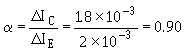
Now take a look at the NPN version of the basic transistor amplifier in figure 2-12 and let's see just how it works.
So far in this discussion, a separate battery has been used to provide the necessary forward-bias voltage. Although a separate battery has been used in the past for convenience, it is not practical to use a battery for emitter-base bias. For instance, it would take a battery slightly over .2 volts to properly forward bias a germanium transistor, while a similar silicon transistor would require a voltage slightly over .6 volts. However, common batteries do not have such voltage values. Also, since bias voltages are quite critical and must be held within a few tenths of one volt, it is easier to work with bias currents flowing through resistors of high ohmic values than with batteries.
By inserting one or more resistors in a circuit, different methods of biasing may be achieved and the emitter-base battery eliminated. In addition to eliminating the battery, some of these biasing methods compensate for slight variations in transistor characteristics and changes in transistor conduction resulting from temperature irregularities. Notice in figure 2-12 that the emitter-base battery has been eliminated and the bias resistor RB has been inserted between the collector and the base. Resistor RB provides the necessary forward bias for the emitter-base junction. Current flows in the emitter-base bias circuit from ground to the emitter, out the base lead, and through RB to VCC. Since the current in the base circuit is very small (a few hundred microamperes) and the forward resistance of the transistor is low, only a few tenths of a volt of positive bias will be felt on the base of the transistor. However, this is enough voltage on the base, along with ground on the emitter and the large positive voltage on the collector, to properly bias the transistor.
Figure 2-12. - The basic transistor amplifier.
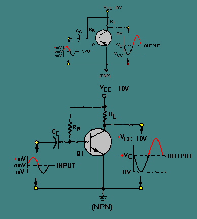
With Q1 properly biased, direct current flows continuously, with or without an input signal, throughout the entire circuit. The direct current flowing through the circuit develops more than just base bias; it also develops the collector voltage (VC) as it flows through Q1 and RL. Notice the collector voltage on the output graph. Since it is present in the circuit without an input signal, the output signal starts at the VC level and either increases or decreases. These dc voltages and currents that exist in the circuit before the application of a signal are known as QUIESCENT voltages and currents (the quiescent state of the circuit).
Resistor RL, the collector load resistor, is placed in the circuit to keep the full effect of the collector supply voltage off the collector. This permits the collector voltage (VC) to change with an input signal, which in turn allows the transistor to amplify voltage. Without RL in the circuit, the voltage on the collector would always be equal to VCC.
The coupling capacitor (CC) is another new addition to the transistor circuit. It is used to pass the ac input signal and block the dc voltage from the preceding circuit. This prevents dc in the circuitry on the left of the coupling capacitor from affecting the bias on Q1. The coupling capacitor also blocks the bias of Q1 from reaching the input signal source.
The input to the amplifier is a sine wave that varies a few millivolts above and below zero. It is introduced into the circuit by the coupling capacitor and is applied between the base and emitter. As the input signal goes positive, the voltage across the emitter-base junction becomes more positive. This in effect increases forward bias, which causes base current to increase at the same rate as that of the input sine wave. Emitter and collector currents also increase but much more than the base current. With an increase in collector current, more voltage is developed across R L. Since the voltage across RL and the voltage across Q1 (collector to emitter) must add up to VCC, an increase in voltage across RL results in an equal decrease in voltage across Q1. Therefore, the output voltage from the amplifier, taken at the collector of Q1 with respect to the emitter, is a negative alternation of voltage that is larger than the input, but has the same sine wave characteristics.
During the negative alternation of the input, the input signal opposes the forward bias. This action decreases base current, which results in a decrease in both emitter and collector currents. The decrease in current through RL decreases its voltage drop and causes the voltage across the transistor to rise along with the output voltage. Therefore, the output for the negative alternation of the input is a positive alternation of voltage that is larger than the input but has the same sine wave characteristics.
By examining both input and output signals for one complete alternation of the input, we can see that the output of the amplifier is an exact reproduction of the input except for the reversal in polarity and the increased amplitude (a few millivolts as compared to a few volts).
The PNP version of this amplifier is shown in the upper part of the figure. The primary difference between the NPN and PNP amplifier is the polarity of the source voltage. With a negative VCC, the PNP base voltage is slightly negative with respect to ground, which provides the necessary forward bias condition between the emitter and base.
When the PNP input signal goes positive, it opposes the forward bias of the transistor. This action cancels some of the negative voltage across the emitter-base junction, which reduces the current through the transistor. Therefore, the voltage across the load resistor decreases, and the voltage across the transistor increases. Since VCC is negative, the voltage on the collector (VC) goes in a negative direction (as shown on the output graph) toward -VCC (for example, from -5 volts to -7 volts). Thus, the output is a negative alternation of voltage that varies at the same rate as the sine wave input, but it is opposite in polarity and has a muchlarger amplitude .
During the negative alternation of the input signal, the transistor current increases because the input voltage aids the forward bias. Therefore, the voltage across RL increases, and consequently, the voltage across the transistor decreases or goes in a positive direction (for example: from -5 volts to -3 volts). This action results in a positive output voltage, which has the same characteristics as the input except that it has been amplified and the polarity is reversed.
In summary, the input signals in the preceding circuits were amplified because the small change in base current caused a large change in collector current. And, by placing resistor RL in series with the collector, voltage amplification was achieved.
TYPES OF BIAS
One of the basic problems with transistor amplifiers is establishing and maintaining the proper values of quiescent current and voltage in the circuit. This is accomplished by selecting the proper circuit-biasing conditions and ensuring these conditions are maintained despite variations in ambient (surrounding) temperature, which cause changes in amplification and even distortion (an unwanted change in a signal). Thus a need arises for a method to properly bias the transistor amplifier and at the same time stabilize its dc operating point (the no signal values of collector voltage and collector current). As mentioned earlier, various biasing methods can be used to accomplish both of these functions. Although there are numerous biasing methods, only three basic types will be considered.
Base-Current Bias (Fixed Bias)
The first biasing method, called BASE CURRENT BIAS or sometimes FIXED BIAS, was used in figure 2-12. As you recall, it consisted basically of a resistor (RB) connected between the collector supply voltage and the base. Unfortunately, this simple arrangement is quite thermally unstable. If the temperature of the transistor rises for any reason (due to a rise in ambient temperature or due to current flow through it), collector current will increase. This increase in current also causes the dc operating point, sometimes called the quiescent or static point, to move away from its desired position (level). This reaction to temperature is undesirable because it affects amplifier gain (the number of times of amplification) and could result in distortion, as you will see later in this discussion.
Self-Bias
A better method of biasing is obtained by inserting the bias resistor directly between the base and collector, as shown in figure 2-13. By tying the collector to the base in this manner, feedback voltage can be fed from the collector to the base to develop forward bias. This arrangement is called SELF-BIAS. Now, if an increase of temperature causes an increase in collector current, the collector voltage (VC) will fall because of the increase of voltage produced across the load resistor (RL). This drop in VC will be fed back to the base and will result in a decrease in the base current. The decrease in base current will oppose the original increase in collector current and tend to stabilize it. The exact opposite effect is produced when the collector current decreases.
Figure 2-13. - A basic transistor amplifier with self-bias.
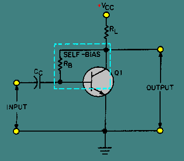
Self-bias has two small drawbacks: (1) It is only partially effective and, therefore, is only used where moderate changes in ambient temperature are expected; (2) it reduces amplification since the signal on the collector also affects the base voltage. This is because the collector and base signals for this particular amplifier configuration are 180 degrees out of phase (opposite in polarity) and the part of the collector signal that is fed back to the base cancels some of the input signal. This process of returning a part of the output back to its input is known as DEGENERATION or NEGATIVE FEEDBACK. Sometimes degeneration is desired to prevent amplitude distortion (an output signal that fails to follow the input exactly) and self-bias may be used for this purpose.
Combination Bias
A combination of fixed and self-bias can be used to improve stability and at the same time overcome some of the disadvantages of the other two biasing methods. One of the most widely used combination-bias systems is the voltage-divider type shown in figure 2-14. Fixed bias is provided in this circuit by the voltage-divider network consisting of R1, R2, and the collector supply voltage (VCC). The dc current flowing through the voltage-divider network biases the base positive with respect to the emitter. Resistor R3, which is connected in series with the emitter, provides the emitter with self-bias. Should IE increase, the voltage drop across R3 would also increase, reducing VC. This reaction to an increase in IE by R3 is another form of degeneration, which results in less output from the amplifier. However, to provide long-term or dc thermal stability, and at the same time, allow minimal ac signal degeneration, the bypass capacitor (Cbp) is placed across R3. If Cbp is large enough, rapid signal variations will not change its charge materially and no degeneration of the signal will occur.
Figure 2-14. - A basic transistor amplifier with combination bias.
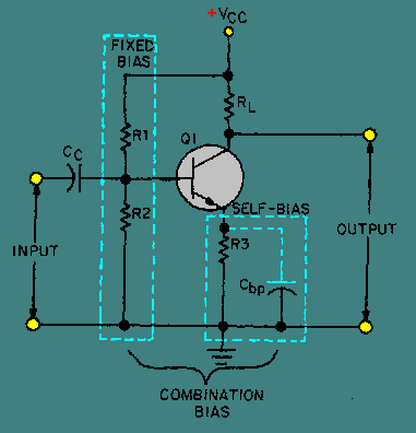
In summary, the fixed-bias resistors, R1 and R2, tend to keep the base bias constant while the emitter bias changes with emitter conduction. This action greatly improves thermal stability and at the same time maintains the correct operating point for the transistor.
AMPLIFIER CLASSES OF OPERATION
In the previous discussions, we assumed that for every portion of the input signal there was an output from the amplifier. This is not always the case with amplifiers. It may be desirable to have the transistor conducting for only a portion of the input signal. The portion of the input for which there is an output determines the class of operation of the amplifier. There are four classes of amplifier operations. They are class A, class AB, class B, and class C.
Class A Amplifier Operation
Class A amplifiers are biased so that variations in input signal polarities occur within the limits of CUTOFF and SATURATION. In a PNP transistor, for example, if the base becomes positive with respect to the emitter, holes will be repelled at the PN junction and no current can flow in the collector circuit. This condition is known as cutoff. Saturation occurs when the base becomes so negative with respect to the emitter that changes in the signal are not reflected in collector-current flow.
Biasing an amplifier in this manner places the dc operating point between cutoff and saturation and allows collector current to flow during the complete cycle (360 degrees) of the input signal, thus providing an output which is a replica of the input. Figure 2-12 is an example of a class A amplifier. Although the output from this amplifier is 180 degrees out of phase with the input, the output current still flows for the complete duration of the input.
The class A operated amplifier is used as an audio- and radio-frequency amplifier in radio, radar, and sound systems, just to mention a few examples.
For a comparison of output signals for the different amplifier classes of operation, refer to figure 2-15 during the following discussion.
Figure 2-15. - A comparison of output signals for the different amplifier classes of operation.
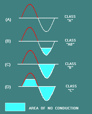
Class AB Amplifier Operation Amplifiers designed for class AB operation are biased so that collector current is zero (cutoff) for a portion of one alternation of the input signal. This is accomplished by making the forward-bias voltage less than the peak value of the input signal. By doing this, the base-emitter junction will be reverse biased during one alternation for the amount of time that the input signal voltage opposes and exceeds the value of forward-bias voltage. Therefore, collector current will flow for more than 180 degrees but less than 360 degrees of the input signal, as shown in figure 2-15 view B. As compared to the class A amplifier, the dc operating point for the class AB amplifier is closer to cutoff.
The class AB operated amplifier is commonly used as a push-pull amplifier to overcome a side effect of class B operation called crossover distortion.
Class B Amplifier Operation
Amplifiers biased so that collector current is cut off during one-half of the input signal are classified class B. The dc operating point for this class of amplifier is set up so that base current is zero with no input signal. When a signal is applied, one half cycle will forward bias the base-emitter junction and IC will flow. The other half cycle will reverse bias the base-emitter junction and IC will be cut off. Thus, for class B operation, collector current will flow for approximately 180 degrees (half) of the input signal, as shown in figure 2-15 view C.
The class B operated amplifier is used extensively for audio amplifiers that require high-power outputs. It is also used as the driver- and power-amplifier stages of transmitters.
Class C Amplifier Operation
In class C operation, collector current flows for less than one half cycle of the input signal, as shown in figure 2-15 view D. The class C operation is achieved by reverse biasing the emitter-base junction, which sets the dc operating point below cutoff and allows only the portion of the input signal that overcomes the reverse bias to cause collector current flow.
The class C operated amplifier is used as a radio-frequency amplifier in transmitters.
From the previous discussion, you can conclude that two primary items determine the class of operation of an amplifier - (1) the amount of bias and (2) the amplitude of the input signal. With a given input signal and bias level, you can change the operation of an amplifier from class A to class B just by removing forward bias. Also, a class A amplifier can be changed to class AB by increasing the input signal amplitude. However, if an input signal amplitude is increased to the point that the transistor goes into saturation and cutoff, it is then called an OVERDRIVEN amplifier.
You should be familiar with two terms used in conjunction with amplifiers - FIDELITY and EFFICIENCY. Fidelity is the faithful reproduction of a signal. In other words, if the output of an amplifier is just like the input except in amplitude, the amplifier has a high degree of fidelity. The opposite of fidelity is a term we mentioned earlier - distortion. Therefore, a circuit that has high fidelity has low distortion. In conclusion, a class A amplifier has a high degree of fidelity. A class AB amplifier has less fidelity, and class B and class C amplifiers have low or "poor" fidelity.
The efficiency of an amplifier refers to the ratio of output-signal power compared to the total input power. An amplifier has two input power sources: one from the signal, and one from the power supply. Since every device takes power to operate, an amplifier that operates for 360 degrees of the input signal uses more power than if operated for 180 degrees of the input signal. By using more power, an amplifier has less power available for the output signal; thus the efficiency of the amplifier is low. This is the case with the class A amplifier. It operates for 360 degrees of the input signal and requires a relatively large input from the power supply. Even with no input signal, the class A amplifier still uses power from the power supply.
Therefore, the output from the class A amplifier is relatively small compared to the total input power. This results in low efficiency, which is acceptable in class A amplifiers because they are used where efficiency is not as important as fidelity.
Class AB amplifiers are biased so that collector current is cut off for a portion of one alternation of the input, which results in less total input power than the class A amplifier. This leads to better efficiency.
Class B amplifiers are biased with little or no collector current at the dc operating point. With no input signal, there is little wasted power. Therefore, the efficiency of class B amplifiers is higher still.
The efficiency of class C is the highest of the four classes of amplifier operations.
TRANSISTOR CONFIGURATIONS
A transistor may be connected in any one of three basic configurations (fig. 2-16): common emitter (CE), common base (CB), and common collector (CC). The term common is used to denote the element that is common to both input and output circuits. Because the common element is often grounded, these configurations are frequently referred to as grounded emitter, grounded base, and grounded collector.
Figure 2-16. - Transistor configurations.
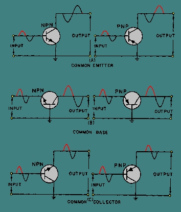
Each configuration, as you will see later, has particular characteristics that make it suitable for specific applications. An easy way to identify a specific transistor configuration is to follow three simple steps:
- Identify the element (emitter, base, or collector) to which the input signal is applied.
- Identify the element (emitter, base, or collector) from which the output signal is taken.
- The remaining element is the common element, and gives the configuration its name.
Therefore, by applying these three simple steps to the circuit in figure 2-12, we can conclude that this circuit is more than just a basic transistor amplifier. It is a common-emitter amplifier.
Common Emitter
The common-emitter configuration (CE) shown in figure 2-16 view A is the arrangement most frequently used in practical amplifier circuits, since it provides good voltage, current, and power gain. The common emitter also has a somewhat low input resistance (500 ohms-1500 ohms), because the input is applied to the forward-biased junction, and a moderately high output resistance (30 kilohms-50 kilohms or more), because the output is taken off the reverse-biased junction. Since the input signal is applied to the base-emitter circuit and the output is taken from the collector-emitter circuit, the emitter is the element common to both input and output.
Since you have already covered what you now know to be a common-emitter amplifier (fig. 2-12), let's take a few minutes and review its operation, using the PNP common-emitter configuration shown in figure 2-16 view A.
When a transistor is connected in a common-emitter configuration, the input signal is injected between the base and emitter, which is a low resistance, low-current circuit. As the input signal swings positive, it also causes the base to swing positive with respect to the emitter. This action decreases forward bias which reduces collector current (IC) and increases collector voltage (making VC more negative). During the negative alternation of the input signal, the base is driven more negative with respect to the emitter. This increases forward bias and allows more current carriers to be released from the emitter, which results in an increase in collector current and a decrease in collector voltage (making VC less negative or swing in a positive direction). The collector current that flows through the high resistance reverse-biased junction also flows through a high resistance load (not shown), resulting in a high level of amplification.
Since the input signal to the common emitter goes positive when the output goes negative, the two signals (input and output) are 180 degrees out of phase. The common-emitter circuit is the only configuration that provides a phase reversal.
The common-emitter is the most popular of the three transistor configurations because it has the best combination of current and voltage gain. The term GAIN is used to describe the amplification capabilities of the amplifier. It is basically a ratio of output versus input. Each transistor configuration gives a different value of gain even though the same transistor is used. The transistor configuration used is a matter of design consideration. However, as a technician you will become interested in this output versus input ratio (gain) to determine whether or not the transistor is working properly in the circuit.
The current gain in the common-emitter circuit is called BETA (b). Beta is the relationship of collector current (output
current) to base current (input current). To calculate beta, use the following formula:

(D is the Greek letter delta, it is used to indicate a small change)
For example, if the input current (IB) in a common emitter changes from 75 mA to 100 mA and the output current (IC) changes from 1.5 mA to 2.6 mA, the current gain (b) will be 44.
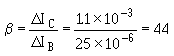
This simply means that a change in base current produces a change in collector current which is 44 times as large.
You may also see the term hfe used in place of b. The terms hfe and b are equivalent and may be used interchangeably. This is because "hfe" means: h = hybrid (meaning mixture)
f = forward current transfer ratio
e = common emitter configuration
e = common emitter configuration
The resistance gain of the common emitter can be found in a method similar to the one used for finding beta:

Once the resistance gain is known, the voltage gain is easy to calculate since it is equal to the current gain (b) multiplied by the resistance gain (E = bR). And, the power gain is equal to the voltage gain multiplied by the current gain b (P = bE).
Common Base
The common-base configuration (CB) shown in figure 2-16, view B is mainly used for impedance matching, since it has a low input resistance (30 ohms-160 ohms) and a high output resistance (250 kilohms-550 kilohms). However, two factors limit its usefulness in some circuit applications: (1) its low input resistance and (2) its current gain of less than 1. Since the CB configuration will give voltage amplification, there are some additional applications, which require both a low-input resistance and voltage amplification, that could use a circuit configuration of this type; for example, some microphone amplifiers.
In the common-base configuration, the input signal is applied to the emitter, the output is taken from the collector, and the base is the element common to both input and output. Since the input is applied to the emitter, it causes the emitter-base junction to react in the same manner as it did in the common-emitter circuit. For example, an input that aids the bias will increase transistor current, and one that opposes the bias will decrease transistor current.
Unlike the common-emitter circuit, the input and output signals in the common-base circuit are in phase. To illustrate this point, assume the input to the PNP version of the common-base circuit in figure 2-16 view B is positive. The signal adds to the forward bias, since it is applied to the emitter, causing the collector current to increase. This increase in Ic results in a greater voltage drop across the load resistor RL (not shown), thus lowering the collector voltage VC. The collector voltage, in becoming less negative, is swinging in a positive direction, and is therefore in phase with the incoming positive signal.
The current gain in the common-base circuit is calculated in a method similar to that of the common emitter except that the input current is I E not IB and the term ALPHA (a) is used in place of beta for gain. Alpha is the relationship of collector current (output current) to emitter current (input current). Alpha is calculated using the formula:

For example, if the input current (IE) in a common base changes from 1 mA to 3 mA and the output current (IC) changes from 1 mA to 2.8 mA, the current gain (a) will be 0.90 or:
This is a current gain of less than 1.
Since part of the emitter current flows into the base and does not appear as collector current, collector current will always be less than the emitter current that causes it. (Remember, IE = IB + IC) Therefore, ALPHA is ALWAYS LESS THAN ONE FOR A
COMMON-BASE CONFIGURATION.
Another term for "a" is hfb. These terms (and hfb) are equivalent and may be used interchangeably. The meaning for the term hfb is derived in the same manner as the term hfe mentioned earlier, except that the last letter "e" has been replaced with "b" to stand for common- base configuration.
Many transistor manuals and data sheets only list transistor current gain characteristics in terms of b or hfe. To find alpha (a) when given beta (b), use the following formula to convert b to a for use with the common-base configuration:

To calculate the other gains (voltage and power) in the common-base configuration when the current gain (a) is known, follow the procedures described earlier under the common-emitter section.
Common Collector
The common-collector configuration (CC) shown in figure 2-16 view C is used mostly for impedance matching. It is also used as a current driver, because of its substantial current gain. It is particularly useful in switching circuitry, since it has the ability to pass signals in either direction (bilateral operation).
In the common-collector circuit, the input signal is applied to the base, the output is taken from the emitter, and the collector is the element common to both input and output. The common collector is equivalent to our old friend the electron-tube cathode follower. Both have high input and low output resistance. The input resistance for the common collector ranges from 2 kilohms to 500 kilohms, and the output resistance varies from 50 ohms to 1500 ohms. The current gain is higher than that in the common emitter, but it has a lower power gain than either the common base or common emitter. Like the common base, the output signal from the common collector is in phase with the input signal. The common collector is also referred to as an emitter-follower because the output developed on the emitter follows the input signal applied to the base.
Transistor action in the common collector is similar to the operation explained for the common base, except that the current gain is not based on the emitter-to-collector current ratio, alpha (a). Instead, it is based on the emitter-to-base current ratio called GAMMA (g), because the output is taken off the emitter. Since a small change in base current controls a large change in emitter current, it is still possible to obtain high current gain in the common collector. However, since the emitter current gain is offset by the low output resistance, the voltage gain is always less than 1 (unity), exactly as in the electron-tube cathode follower
The common-collector current gain, gamma (g), is defined as

and is related to collector-to-base current gain, beta (b), of the common-emitter circuit by the formula:
Since a given transistor may be connected in any of three basic configurations, there is a definite relationship, as pointed out earlier, between alpha (a), beta (b), and gamma (g). These relationships are listed again for your convenience:
Take, for example, a transistor that is listed on a manufacturer's data sheet as having an alpha of 0.90. We wish to use it in a common emitter configuration. This means we must find beta. The calculations are:
Therefore, a change in base current in this transistor will produce a change in collector current that will be 9 times as large.
If we wish to use this same transistor in a common collector, we can find gamma (g) by:
To summarize the properties of the three transistor configurations, a comparison chart is provided in table 2-1 for your convenience.
Table 2-1. - Transistor Configuration Comparison Chart
| AMPLIFIER TYPE | COMMON BASE | COMMON EMITTER | COMMON COLLECTOR |
| INPUT/OUTPUT PHASE RELATIONSHIP | 0° | 180° | 0° |
| VOLTAGE GAIN | HIGH | MEDIUM | LOW |
| CURRENT GAIN | LOW(a) | MEDIUM(b) | HIGH(g) |
| POWER GAIN | LOW | HIGH | MEDIUM |
| INPUT RESISTANCE | LOW | MEDIUM | HIGH |
| OUTPUT RESISTANCE | HIGH | MEDIUM | LOW |
Now that we have analyzed the basic transistor amplifier in terms of bias, class of operation, and circuit configuration, let's apply what has been covered to figure 2-12. A reproduction of figure 2-12 is shown below for your convenience.
This illustration is not just the basic transistor amplifier shown earlier in figure 2-12 but a class A amplifier configured as a common emitter using fixed bias. From this, you should be able to conclude the following:
- Because of its fixed bias, the amplifier is thermally unstable.
- Because of its class A operation, the amplifier has low efficiency but good fidelity.
- Because it is configured as a common emitter, the amplifier has good voltage, current, and power gain.
In conclusion, the type of bias, class of operation, and circuit configuration are all clues to the function and possible application of the amplifier.
TRANSISTOR SPECIFICATIONS
Transistors are available in a large variety of shapes and sizes, each with its own unique characteristics. The characteristics for each of these transistors are usually presented on SPECIFICATION SHEETS or they may be included in transistor manuals. Although many properties of a transistor could be specified on these sheets, manufacturers list only some of them. The specifications listed vary with different manufacturers, the type of transistor, and the application of the transistor. The specifications usually cover the following items.
A general description of the transistor that includes the following information:
- The kind of transistor. This covers the material used, such as germanium or silicon; the type of transistor(NPN or PNP); and the construction of the transistor(whether alloy-junction, grown, or diffused junction, etc.).
- Some of the common applications for the transistor, such as audio amplifier, oscillator, rf amplifier, etc.
- General sales features, such as size and packaging(mechanical data).
The "Absolute Maximum Ratings" of the transistor are the direct voltage and current values that if exceeded in operation may result in transistor failure. Maximum ratings usually include collector-to-base voltage, emitter-to-base voltage, collector current, emitter current, and collector power dissipation. The typical operating values of the transistor. These values are presented only as a guide. The values vary widely, are dependent upon operating voltages, and also upon which element is common in the circuit. The values listed may include collector-emitter voltage, collector current, input resistance, load resistance, current-transfer ratio(another name for alpha or beta), and collector cutoff current, which is leakage current from collector to base when no emitter current is applied. Transistor characteristic curves may also be included in this section. A transistor characteristic curve is a graph plotting the relationship between currents and voltages in a circuit.
More than one curve on a graph is called a "family of curves." Additional information for engineering-design purposes.
So far, many letter symbols, abbreviations, and terms have been introduced, some frequently used and others only rarely used.
For a complete list of all semiconductor letter symbols and terms, refer to EIMB series 000-0140, Section III.
Transistors can be identified by a Joint Army-Navy (JAN) designation printed directly on the case of the transistor. The marking scheme explained earlier for diodes is also used for transistor identification. The first number indicates the number of junctions. The letter "N" following the first number tells us that the component is a semiconductor. And, the 2- or 3-digit number following the N is the manufacturer's identification number. If the last number is followed by a letter, it indicates a later, improved version of the device. For example, a semiconductor designated as type 2N130A signifies a three-element transistor of semiconductor material that is an improved version of type 130:
| 2 | N | 130 |
| A NUMBER OF JUNCTIONS (TRANSISTOR) | SEMI-CONDUCTOR IDENTIFICATION | NUMBER FIRST MODIFICATION |
You may also find other markings on transistors that do not relate to the JAN marking system. These markings are manufacturers' identifications and may not conform to a standardized system. If in doubt, always replace a transistor with one having identical markings. To ensure that an identical replacement or a correct substitute is used, consult an equipment or transistor manual for specifications on the transistor.
TRANSISTOR MAINTENANCE
Transistors are very rugged and are expected to be relatively trouble free. Encapsulation and conformal coating techniques now in use promise extremely long life expectancies. In theory, a transistor should last indefinitely. However, if transistors are subjected to current overloads, the junctions will be damaged or even destroyed. In addition, the application of excessively high operating voltages can damage or destroy the junctions through arc-over or excessive reverse currents. One of the greatest dangers to the transistor is heat, which will cause excessive current flow and eventual destruction of the transistor.
To determine if a transistor is good or bad, you can check it with an ohmmeter or a transistor tester. In many cases, you can substitute a transistor known to be good for one that is questionable and thus determine the condition of a suspected transistor. This method of testing is highly accurate and sometimes the quickest, but it should be used only after you make certain that there are no circuit defects that might damage the replacement transistor. If more than one defective transistor is present in the equipment where the trouble has been localized, this testing method becomes cumbersome, as several transistors may have to be replaced before the trouble is corrected. To determine which stages failed and which transistors are not defective, all the removed transistors must be tested. This test can be made by using a standard Navy ohmmeter, transistor tester, or by observing whether the equipment operates correctly as each of the removed transistors is reinserted into the equipment. A word of caution-indiscriminate substitution of transistors in critical circuits should be avoided.
When transistors are soldered into equipment, substitution is not practicable; it is generally desirable to test these transistors in their circuits.
Freddy R Vallenilla R
16.791.006
CAF
No hay comentarios:
Publicar un comentario