An often-used circuit applying the bipolar junction transistor is the so-called current mirror, which serves as a simple current regulator, supplying nearly constant current to a load over a wide range of load resistances.
We know that in a transistor operating in its active mode, collector current is equal to base current multiplied by the ratio β. We also know that the ratio between collector current and emitter current is called α. Because collector current is equal to base current multiplied by β, and emitter current is the sum of the base and collector currents, α should be mathematically derivable from β. If you do the algebra, you'll find that α = β/(β+1) for any transistor.
We've seen already how maintaining a constant base current through an active transistor results in the regulation of collector current, according to the β ratio. Well, the α ratio works similarly: if emitter current is held constant, collector current will remain at a stable, regulated value so long as the transistor has enough collector-to-emitter voltage drop to maintain it in its active mode. Therefore, if we have a way of holding emitter current constant through a transistor, the transistor will work to regulate collector current at a constant value.
Remember that the base-emitter junction of a BJT is nothing more than a PN junction, just like a diode, and that the "diode equation" specifies how much current will go through a PN junction given forward voltage drop and junction temperature:
If both junction voltage and temperature are held constant, then the PN junction current will be constant. Following this rationale, if we were to hold the base-emitter voltage of a transistor constant, then its emitter current will be constant, given a constant temperature. (Figure below)

Constant VBE gives constant IB, constant IE, and constant IC.
This constant emitter current, multiplied by a constant α ratio, gives a constant collector current through Rload, if enough battery voltage is available to keep the transistor in its active mode for any change in Rload's resistance.
To maintain a constant voltage across the transistor's base-emitter junction use a forward-biased diode to establish a constant voltage of approximately 0.7 volts, and connect it in parallel with the base-emitter junction as in Figure below.

Diode junction 0.7 V maintains constant base voltage, and constant base current.
The voltage dropped across the diode probably won't be 0.7 volts exactly. The exact amount of forward voltage dropped across it depends on the current through the diode, and the diode's temperature, all in accordance with the diode equation. If diode current is increased (say, by reducing the resistance of Rbias), its voltage drop will increase slightly, increasing the voltage drop across the transistor's base-emitter junction, which will increase the emitter current by the same proportion, assuming the diode's PN junction and the transistor's base-emitter junction are well-matched to each other. In other words, transistor emitter current will closely equal diode current at any given time. If you change the diode current by changing the resistance value of Rbias, then the transistor's emitter current will follow suit, because the emitter current is described by the same equation as the diode's, and both PN junctions experience the same voltage drop.
Remember, the transistor's collector current is almost equal to its emitter current, as the α ratio of a typical transistor is almost unity (1). If we have control over the transistor's emitter current by setting diode current with a simple resistor adjustment, then we likewise have control over the transistor's collector current. In other words, collector current mimics, or mirrors, diode current.
Current through resistor Rload is therefore a function of current set by the bias resistor, the two being nearly equal. This is the function of the current mirror circuit: to regulate current through the load resistor by conveniently adjusting the value of Rbias. Current through the diode is described by a simple equation: power supply voltage minus diode voltage (almost a constant value), divided by the resistance of Rbias.
To better match the characteristics of the two PN junctions (the diode junction and the transistor base-emitter junction), a transistor may be used in place of a regular diode, as in Figure below (a).
 |  |
Current mirror circuits.
Because temperature is a factor in the "diode equation," and we want the two PN junctions to behave identically under all operating conditions, we should maintain the two transistors at exactly the same temperature. This is easily done using discrete components by gluing the two transistor cases back-to-back. If the transistors are manufactured together on a single chip of silicon (as a so-called integrated circuit, or IC), the designers should locate the two transistors close to one another to facilitate heat transfer between them.
The current mirror circuit shown with two NPN transistors in Figure above (a) is sometimes called a current-sinking type, because the regulating transistor conducts current to the load from ground ("sinking" current), rather than from the positive side of the battery ("sourcing" current). If we wish to have a grounded load, and a current sourcing mirror circuit, we may use PNP transistors like Figure above (b).
While resistors can be manufactured in ICs, it is easier to fabricate transistors. IC designers avoid some resistors by replacing load resistors with current sources. A circuit like an operational amplifier built from discrete components will have a few transistors and many resistors. An integrated circuit version will have many transistors and a few resistors. In Figure below One voltage reference, Q1, drives multiple current sources: Q2, Q3, and Q4. If Q2 and Q3 are equal area transistors the load currents Iload will be equal. If we need a 2·Iload, parallel Q2 and Q3. Better yet fabricate one transistor, say Q3 with twice the area of Q2. Current I3 will then be twice I2. In other words, load current scales with transistor area.
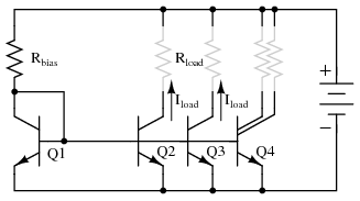
Multiple current mirrors may be slaved from a single (Q1 - Rbias) voltage source.
Note that it is customary to draw the base voltage line right through the transistor symbols for multiple current mirrors! Or in the case of Q4 in Figure above, two current sources are associated with a single transistor symbol. The load resistors are drawn almost invisible to emphasize the fact that these do not exist in most cases. The load is often another (multiple) transistor circuit, say a pair of emitters of a differential amplifier, for example Q3 and Q4 in "A simple operational amplifier", Ch 8 . Often, the collector load of a transistor is not a resistor but a current mirror. For example the collector load of Q4 collector , Ch 8 is a current mirror (Q2).
For an example of a current mirror with multiple collector outputs see Q13 in the model 741 op-amp , Ch 8 . The Q13 current mirror outputs substitute for resistors as collector loads for Q15 and Q17. We see from these examples that current mirrors are preferred as loads over resistors in integrated circuitry.
Transistor ratings and packages
Like all electrical and electronic components, transistors are limited in the amounts of voltage and current each one can handle without sustaining damage. Since transistors are more complex than some of the other components you're used to seeing at this point, these tend to have more kinds of ratings. What follows is an itemized description of some typical transistor ratings.
Power dissipation: When a transistor conducts current between collector and emitter, it also drops voltage between those two points. At any given time, the power dissipated by a transistor is equal to the product (multiplication) of collector current and collector-emitter voltage. Just like resistors, transistors are rated for how many watts each can safely dissipate without sustaining damage. High temperature is the mortal enemy of all semiconductor devices, and bipolar transistors tend to be more susceptible to thermal damage than most. Power ratings are always referenced to the temperature of ambient (surrounding) air. When transistors are to be used in hotter environments (>25o, their power ratings must be derated to avoid a shortened service life.
Reverse voltages: As with diodes, bipolar transistors are rated for maximum allowable reverse-bias voltage across their PN junctions. This includes voltage ratings for the emitter-base junction VEB , collector-base junction VCB , and also from collector to emitter VCE .
VEB , the maximum reverse voltage from emitter to base is approximately 7 V for some small signal transistors. Some circuit designers use discrete BJTs as 7 V zener diodes with a series current limiting resistor. Transistor inputs to analog integrated circuits also have a VEB rating, which if exceeded will cause damage, no zenering of the inputs is allowed.
The rating for maximum collector-emitter voltage VCE can be thought of as the maximum voltage it can withstand while in full-cutoff mode (no base current). This rating is of particular importance when using a bipolar transistor as a switch. A typical value for a small signal transistor is 60 to 80 V. In power transistors, this could range to 1000 V, for example, a horizontal deflection transistor in a cathode ray tube display.
Collector current: A maximum value for collector current IC will be given by the manufacturer in amps. Typical values for small signal transistors are 10s to 100s of mA, 10s of A for power transistors. Understand that this maximum figure assumes a saturated state (minimum collector-emitter voltage drop). If the transistor is not saturated, and in fact is dropping substantial voltage between collector and emitter, the maximum power dissipation rating will probably be exceeded before the maximum collector current rating. Just something to keep in mind when designing a transistor circuit!
Saturation voltages: Ideally, a saturated transistor acts as a closed switch contact between collector and emitter, dropping zero voltage at full collector current. In reality this is never true. Manufacturers will specify the maximum voltage drop of a transistor at saturation, both between the collector and emitter, and also between base and emitter (forward voltage drop of that PN junction). Collector-emitter voltage drop at saturation is generally expected to be 0.3 volts or less, but this figure is of course dependent on the specific type of transistor. Low voltage transistors, low VCE , show lower saturation voltages. The saturation voltage is also lower for higher base drive current.
Base-emitter forward voltage drop, kVBE , is similar to that of an equivalent diode, ≅0.7 V, which should come as no surprise.
Beta: The ratio of collector current to base current, β is the fundamental parameter characterizing the amplifying ability of a bipolar transistor. β is usually assumed to be a constant figure in circuit calculations, but unfortunately this is far from true in practice. As such, manufacturers provide a set of β (or "hfe") figures for a given transistor over a wide range of operating conditions, usually in the form of maximum/minimum/typical ratings. It may surprise you to see just how widely β can be expected to vary within normal operating limits. One popular small-signal transistor, the 2N3903, is advertised as having a β ranging from 15 to 150 depending on the amount of collector current. Generally, β is highest for medium collector currents, decreasing for very low and very high collector currents. hfe is small signal AC gain; hFE is large AC signal gain or DC gain.
Alpha: the ratio of collector current to emitter current, α=IC/IE . α may be derived from β, being α=β/(β+1) .
Bipolar transistors come in a wide variety of physical packages. Package type is primarily dependent upon the required power dissipation of the transistor, much like resistors: the greater the maximum power dissipation, the larger the device has to be to stay cool. Figure below shows several standardized package types for three-terminal semiconductor devices, any of which may be used to house a bipolar transistor. There are many other semiconductor devices other than bipolar transistors which have three connection points. Note that the pin-outs of plastic transistors can vary within a single package type, e.g. TO-92 in Figure below. It is impossible to positively identify a three-terminal semiconductor device without referencing the part number printed on it, or subjecting it to a set of electrical tests.

Transistor packages, dimensions in mm.
Small plastic transistor packages like the TO-92 can dissipate a few hundred milliwatts. The metal cans, TO-18 and TO-39 can dissipate more power, several hundred milliwatts. Plastic power transistor packages like the TO-220 and TO-247 dissipate well over 100 watts, approaching the dissipation of the all metal TO-3. The dissipation ratings listed in Figure above are the maximum ever encountered by the author for high powered devices. Most power transistors are rated at half or less than the listed wattage. Consult specific device datasheets for actual ratings. The the semiconductor die in the TO-220 and TO-247 plastic packages is mounted to a heat conductive metal slug which transfers heat from the back of the package to a metal heatsink, not shown. A thin coating of thermally conductive grease is applied to the metal before mounting the transistor to the heatsink. Since the TO-220 and TO-247 slugs, and the TO-3 case are connected to the collector, it is sometimes necessary to electrically isolate the these from a grounded heatsink by an interposed mica or polymer washer. The datasheet ratings for the power packages are only valid when mounted to a heatsink. Without a heatsink, a TO-220 dissipates approximately 1 watt safely in free air.
Datasheet maximum power disipation ratings are difficult to acheive in practice. The maximum power dissipation is based on a heatsink maintaining the transistor case at no more than 25oC. This is difficult with an air cooled heatsink. The allowable power dissipation decreases with increasing temperature. This is known as derating. Many power device datasheets include a dissipation versus case termperaure graph.
BJT quirks
An ideal transistor would show 0% distortion in amplifying a signal. Its gain would extend to all frequencies. It would control hundreds of amperes of current, at hundreds of degrees C. In practice, available devices show distortion. Amplification is limited at the high frequency end of the spectrum. Real parts only handle tens of amperes with precautions. Care must be taken when paralleling transistors for higher current. Operation at elevated temperatures can destroy transistors if precautions are not taken.
Nonlinearity
The class A common-emitter amplifier (similar to Figure previous)is driven almost to clipping in Figure below . Note that the positive peak is flatter than the negative peaks. This distortion distortion is unacceptable in many applications like high-fidelity audio.

Distortion in large signal common-emitter amplifier.
Small signal amplifiers are relatively linear because they use a small linear section of the transistor characteristics. Large signal amplifiers are not 100% linear because transistor characteristics like β are not constant, but vary with collector current. β is high at low collector current, and low at very low current or high current. Though, we primarily encounter decreasing β with increasing collector current.
common-emitter amplifier Vbias 4 0 0.74 Vsig 5 4 sin (0 125m 2000 0 0) rbias 6 5 2k q1 2 6 0 q2n2222 r 3 2 1000 v1 3 0 dc 10 .model q2n2222 npn (is=19f bf=150 + vaf=100 ikf=0.18 ise=50p ne=2.5 br=7.5 + var=6.4 ikr=12m isc=8.7p nc=1.2 rb=50 + re=0.4 rc=0.3 cje=26p tf=0.5n + cjc=11p tr=7n xtb=1.5 kf=0.032f af=1) .fourier 2000 v(2) .tran 0.02m 0.74m .end | spice -b ce.cir Fourier analysis v(2): THD: 10.4688 % Har Freq Norm Mag --- ---- --------- 0 0 0 1 2000 1 2 4000 0.0979929 3 6000 0.0365461 4 8000 0.00438709 5 10000 0.00115878 6 12000 0.00089388 7 14000 0.00021169 8 16000 3.8158e-05 9 18000 3.3726e-05 |
SPICE net list: for transient and fourier analyses. Fourier analysis shows 10% total harmonic distortion (THD).
The SPICE listing in Table above illustrates how to quantify the amount of distortion. The ".fourier 2000 v(2)" command tells SPICE to perm a fourier analysis at 2000 Hz on the output v(2). At the command line "spice -b circuitname.cir" produces the Fourier analysis output in Table above. It shows THD (total harmonic distortion) of over 10%, and the contribution of the individual harmonics.
A partial solution to this distortion is to decrease the collector current or operate the amplifier over a smaller portion of the load line. The ultimate solution is to apply negative feedback.
Temperature drift
Temperature affects the AC and DC characteristics of transistors. The two aspects to this problem are environmental temperature variation and self-heating. Some applications, like military and automotive, require operation over an extended temperature range. Circuits in a benign environment are subject to self-heating, in particular high power circuits.
Leakage current ICO and β increase with temperature. The DC β hFE increases exponentially. The AC β hfe increases, but not as rapidly. It doubles over the range of -55o to 85o C. As temperature increases, the increase in hfe will yield a larger common-emitter output, which could be clipped in extreme cases. The increase in hFE shifts the bias point, possibly clipping one peak. The shift in bias point is amplified in multi-stage direct-coupled amplifiers. The solution is some form of negative feedback to stabilize the bias point. This also stabilizes AC gain.
Increasing temperature in Figure below (a) will decrease VBE from the nominal 0.7V for silicon transistors. Decreasing VBE increases collector current in a common-emitter amplifier, further shifting the bias point. The cure for shifting VBE is a pair of transistors configured as a differential amplifier. If both transistors in Figure below (b) are at the same temperature, the VBE will track with changing temperature and cancel.

(a) single ended CE amplifier vs (b) differential amplifier with VBE cancellation.
The maximum recommended junction temperature for silicon devices is frequently 125o C. Though, this should be derated for higher reliability. Transistor action ceases beyond 150o C. Silicon carbide and diamond transistors will operate considerably higher.
Thermal runaway
The problem with increasing temperature causing increasing collector current is that more current increase the power dissipated by the transistor which, in turn, increases its temperature. This self-reinforcing cycle is known as thermal run away, which may destroy the transistor. Again, the solution is a bias scheme with some form of negative feedback to stabilize the bias point.
Junction capacitance
Capacitance exists between the terminals of a transistor. The collector-base capacitance CCB and emitter-base capacitance CEB decrease the gain of a common emitter circuit at higher frequencies.
In a common emitter amplifier, the capacitive feedback from collector to base effectively multiplies CCB by β. The amount of negative gain-reducing feedback is related to both current gain, and amount of collector-base capacitance. This is known as the Miller effect, Miller effect.
Noise
The ultimate sensitivity of small signal amplifiers is limited by noise due to random variations in current flow. The two major sources of noise in transistors are shot noise due to current flow of carriers in the base and thermal noise. The source of thermal noise is device resistance and increases with temperature:

Noise in a transistor amplifier is defined in terms of excess noise generated by the amplifier, not that noise amplified from input to output, but that generated within the amplifier. This is determined by measuring the signal to noise ratio (S/N) at the amplifier input and output. The AC voltage output of an amplifier with a small signal input corresponds to S+N, signal plus noise. The AC voltage with no signal in corresponds to noise N. The noise figure F is defined in terms of S/N of amplifier input and output:

The noise figure F for RF (radio frequency) transistors is usually listed on transistor data sheets in decibels, FdB. A good VHF (very high frequency, 30 MHz to 300 Mhz) noise figure is < 1 dB. The noise figure above VHF increases considerable, 20 dB per decade as shown in Figure below.

Small signal transistor noise figure vs Frequency. After Thiele, Figure 11.147 [AGT]
Figure above also shows that noise at low frequencies increases at 10 dB per decade with decreasing frequency. This noise is known as 1/f noise.
Noise figure varies with the transistor type (part number). Small signal RF transistors used at the antenna input of a radio receiver are specifically designed for low noise figure. Noise figure varies with bias current and impedance matching. The best noise figure for a transistor is achieved at lower bias current, and possibly with an impedance mismatch.
Thermal mismatch (problem with paralleling transistors)
If two identical power transistors were paralleled for higher current, one would expect them to share current equally. Because of differences in characteristerics, transistors do not share current equally.

Transistors paralleled for increased power require emitter ballast resistors
It is not practical to select identical transistors. The β for small signal transistors typically has a range of 100-300, power transistors: 20-50. If each one could be matched, one still might run hotter than the other due to environmental conditions. The hotter transistor draws more current resulting in thermal runaway. The solution when paralleling bipolar transistors is to insert emitter resistors known as ballast resistors of less than an ohm. If the hotter transistor draws more current, the voltage drop across the ballast resistor increases— negative feedback. This decreases the current. Mounting all transistors on the same heatsink helps equalize current too.
High frequency effects
The performance of a transistor amplifier is relatively constant, up to a point, as shown by the small signal common-emitter current gain with increasing frequency in Figure below. Beyond that point the performance of a transistor degrades as frequency increases.
Beta cutoff frequency, fT is the frequency at which common-emitter small signal current gain (hfe) falls to unity. (Figure below) A practical amplifier must have a gain >1. Thus, a transistor cannot be used in a practical amplifier at fT. A more useable limit for a transistor is 0.1·fT.

Common-emitter small signal current gain (hfe) vs frequency.
Some RF silicon bipolar transistors are useable as amplifers up to a few GHz. Silicon-germanium devices extend the upper range to 10 GHz.
Alpha cutoff frequency, falpha is the frequency at which the α falls to 0.707 of low frequency α,0 α=0.707α0. Alpha cutoff and beta cutoff are nearly equal: falpha≅fT Beta cutoff fT is the preferred figure of merit of high frequency performance.
fmax is the highest frequency of oscillation possible under the most favorable conditions of bias and impedance matching. It is the frequency at which the power gain is unity. All of the output is fed back to the input to sustain oscillations. fmax is an upper limit for frequency of operation of a transistor as an active device. Though, a practical amplifier would not be useable at fmax.
Miller effect: The high frequency limit for a transistor is related to the junction capacitances. For example a PN2222A has an input capacitance Cobo=9pF and an output capacitance Cibo=25pF from C-B and E-B respectively. [FAR] Although the C-E capacitance of 25 pF seems large, it is less of a factor than the C-B (9pF) capacitance. because of the Miller effect, the C-B capacitance has an effect on the base equivalent to beta times the capacitance in the common-emitter amplifier. Why might this be? A common-emitter amplifier inverts the signal from base to collector. The inverted collector signal fed back to the base opposes the input on the base. The collector signal is beta times larger than the input. For the PN2222A, β=50–300. Thus, the 9pF C-E capacitance looks like 9·50=450pF to 9·300=2700pF.
The solution to the junction capacitance problem is to select a high frequency transistor for wide bandwidth applications— RF (radio frequency) or microwave transistor. The bandwidth can be extended further by using the common-base instead of the common-emitter configuration. The grounded base shields the emitter input from capacitive collector feedback. A two-transistor cascode arrangement will yield the same bandwidth as the common-base, with the higher input impedance of the common-emitter.
Freddy R Vallenilla R
16.791.006
CAF
No hay comentarios:
Publicar un comentario