While the C-B (common-base) amplifier is known for wider bandwidth than the C-E (common-emitter) configuration, the low input impedance (10s of Ω) of C-B is a limitation for many applications. The solution is to precede the C-B stage by a low gain C-E stage which has moderately high input impedance (kΩs). See Figure below. The stages are in a cascode configuration, stacked in series, as opposed to cascaded for a standard amplifier chain. See "Capacitor coupled three stage common-emitter amplifier" Capacitor coupled for a cascade example. The cascode amplifier configuration has both wide bandwidth and a moderately high input impedance.

The cascode amplifier is combined common-emitter and common-base. This is an AC circuit equivalent with batteries and capacitors replaced by short circuits.
The key to understanding the wide bandwidth of the cascode configuration is the Miller effect Miller effect. It is the multiplication of the bandwidth robbing collector-base capacitance by beta. This C-B capacitance is smaller than the E-B capacitance. Thus, one would think that the C-B capacitance would have little effect. However, in the C-E configuration, the collector output signal is out of phase with the input at the base. The collector signal capacitively coupled back opposes the base signal. Moreover, the collector feedback is beta times larger than the base signal. Thus, the small C-B capacitance appears beta times larger than its actual value. This capacitive gain reducing feedback increases with frequency, reducing the high frequency response of a C-E amplifier.
A common-base configuration is not subject to the Miller effect because the grounded base shields the collector signal from being fed back to the emitter input. Thus, a C-B amplifier has better high frequency response. To have a moderately high input impedance, the C-E stage is still desirable. The key is to reduce the gain (to about 1) of the C-E stage to reduce the Miller effect C-B feedback to 1·CCB. The total C-B feedback is the Miller capacitance 1·CCB plus the actual capacitance CCB for a total of 2·CCB. This is a considerable reduction from β·CCB.
The way to reduce the common-emitter gain is to reduce the load resistance. The gain of a C-E amplifier is approximately RC/RE. The internal emitter resistance REE at 1mA emitter current is 26Ω. For details on the 26Ω, see "Derivation of REE". The collector load RC is the resistance of the emitter of the C-B stage loading the C-E stage, 26Ω again. CE gain amplifier gain is approximately RC/RE=26/26=1. We now have a moderately high input impedance C-E stage without suffering the Miller effect, but no dB voltage gain. The C-B stage provides a high voltage gain. Thus, the cascode has moderately high input impedance of the CE, good gain, and good bandwidth of the C-B.
SPICE: Cascode and common-emitter for comparison.
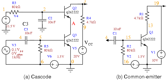
The SPICE version of both a cascode amplifier, and for comparison, a common-emitter amplifier is shown in Figure above. The netlist is in Table below. The AC source V3 drives both amplifiers via node 4. The bias resistors for this circuit are calculated in an example problem cascode.

SPICE waveforms. Note that Input is multiplied by 10 for visibility.
SPICE netlist for printing AC input and output voltages.
*SPICE circuit <03502.eps> from XCircuit v3.20 V1 19 0 10 Q1 13 15 0 q2n2222 Q2 3 2 A q2n2222 R1 19 13 4.7k V2 16 0 1.5 C1 4 15 10n R2 15 16 80k Q3 A 5 0 q2n2222 V3 4 6 SIN(0 0.1 1k) ac 1 R3 1 2 80k R4 3 9 4.7k C2 2 0 10n C3 4 5 10n R5 5 6 80k V4 1 0 11.5 V5 9 0 20 V6 6 0 1.5 .model q2n2222 npn (is=19f bf=150 + vaf=100 ikf=0.18 ise=50p ne=2.5 br=7.5 + var=6.4 ikr=12m isc=8.7p nc=1.2 rb=50 + re=0.4 rc=0.3 cje=26p tf=0.5n + cjc=11p tr=7n xtb=1.5 kf=0.032f af=1) .tran 1u 5m .AC DEC 10 1k 100Meg .end
The waveforms in Figure above show the operation of the cascode stage. The input signal is displayed multiplied by 10 so that it may be shown with the outputs. Note that both the Cascode, Common-emitter, and Va (intermediate point) outputs are inverted from the input. Both the Cascode and Common emitter have large amplitude outputs. The Va point has a DC level of about 10V, about half way between 20V and ground. The signal is larger than can be accounted for by a C-E gain of 1, It is three times larger than expected.

Cascode vs common-emitter banwidth.
Figure above shows the frequency response to both the cascode and common-emitter amplifiers. The SPICE statements responsible for the AC analysis, extracted from the listing:
V3 4 6 SIN(0 0.1 1k) ac 1 .AC DEC 10 1k 100Meg
Note the "ac 1" is necessary at the end of the V3 statement. The cascode has marginally better mid-band gain. However, we are primarily looking for the bandwidth measured at the -3dB points, down from the midband gain for each amplifier. This is shown by the vertical solid lines in Figure above. It is also possible to print the data of interest from nutmeg to the screen, the SPICE graphical viewer (command, first line):
nutmeg 6 -> print frequency db(vm(3)) db(vm(13)) Index frequency db(vm(3)) db(vm(13)) 22 0.158MHz 47.54 45.41 33 1.995MHz 46.95 42.06 37 5.012MHz 44.63 36.17
Index 22 gives the midband dB gain for Cascode vm(3)=47.5dB and Common-emitter vm(13)=45.4dB. Out of many printed lines, Index 33 was the closest to being 3dB down from 45.4dB at 42.0dB for the Common-emitter circuit. The corresponding Index 33 frequency is approximately 2Mhz, the common-emitter bandwidth. Index 37 vm(3)=44.6db is approximately 3db down from 47.5db. The corresponding Index37 frequency is 5Mhz, the cascode bandwidth. Thus, the cascode amplifier has a wider bandwidth. We are not concerned with the low frequency degradation of gain. It is due to the capacitors, which could be remedied with larger ones.
The 5MHz bandwith of our cascode example, while better than the common-emitter example, is not exemplary for an RF (radio frequency) amplifier. A pair of RF or microwave transistors with lower interelectrode capacitances should be used for higher bandwidth. Before the invention of the RF dual gate MOSFET, the BJT cascode amplifier could have been found in UHF (ultra high frequency) TV tuners.
Biasing techniques
In the common-emitter section of this chapter, we saw a SPICE analysis where the output waveform resembled a half-wave rectified shape: only half of the input waveform was reproduced, with the other half being completely cut off. Since our purpose at that time was to reproduce the entire waveshape, this constituted a problem. The solution to this problem was to add a small bias voltage to the amplifier input so that the transistor stayed in active mode throughout the entire wave cycle. This addition was called a bias voltage.
A half-wave output is not problematic for some applications. In fact, some applications may necessitate this very kind of amplification. Because it is possible to operate an amplifier in modes other than full-wave reproduction and specific applications require different ranges of reproduction, it is useful to describe the degree to which an amplifier reproduces the input waveform by designating it according to class. Amplifier class operation is categorized with alphabetical letters: A, B, C, and AB.
For Class A operation, the entire input waveform is faithfully reproduced. Although I didn't introduce this concept back in the common-emitter section, this is what we were hoping to attain in our simulations. Class A operation can only be obtained when the transistor spends its entire time in the active mode, never reaching either cutoff or saturation. To achieve this, sufficient DC bias voltage is usually set at the level necessary to drive the transistor exactly halfway between cutoff and saturation. This way, the AC input signal will be perfectly "centered" between the amplifier's high and low signal limit levels.

Class A: The amplifier output is a faithful reproduction of the input.
Class B operation is what we had the first time an AC signal was applied to the common-emitter amplifier with no DC bias voltage. The transistor spent half its time in active mode and the other half in cutoff with the input voltage too low (or even of the wrong polarity!) to forward-bias its base-emitter junction.

Class B: Bias is such that half (180o) of the waveform is reproduced.
By itself, an amplifier operating in class B mode is not very useful. In most circumstances, the severe distortion introduced into the waveshape by eliminating half of it would be unacceptable. However, class B operation is a useful mode of biasing if two amplifiers are operated as a push-pull pair, each amplifier handling only half of the waveform at a time:

Class B push pull amplifier: Each transistor reproduces half of the waveform. Combining the halves produces a faithful reproduction of the whole wave.
Transistor Q1 "pushes" (drives the output voltage in a positive direction with respect to ground), while transistor Q2 "pulls" the output voltage (in a negative direction, toward 0 volts with respect to ground). Individually, each of these transistors is operating in class B mode, active only for one-half of the input waveform cycle. Together, however, both function as a team to produce an output waveform identical in shape to the input waveform.
A decided advantage of the class B (push-pull) amplifier design over the class A design is greater output power capability. With a class A design, the transistor dissipates considerable energy in the form of heat because it never stops conducting current. At all points in the wave cycle it is in the active (conducting) mode, conducting substantial current and dropping substantial voltage. There is substantial power dissipated by the transistor throughout the cycle. In a class B design, each transistor spends half the time in cutoff mode, where it dissipates zero power (zero current = zero power dissipation). This gives each transistor a time to "rest" and cool while the other transistor carries the burden of the load. Class A amplifiers are simpler in design, but tend to be limited to low-power signal applications for the simple reason of transistor heat dissipation.
Another class of amplifier operation known as class AB, is somewhere between class A and class B: the transistor spends more than 50% but less than 100% of the time conducting current.
If the input signal bias for an amplifier is slightly negative (opposite of the bias polarity for class A operation), the output waveform will be further "clipped" than it was with class B biasing, resulting in an operation where the transistor spends most of the time in cutoff mode:

Class C: Conduction is for less than a half cycle (< 180o).
At first, this scheme may seem utterly pointless. After all, how useful could an amplifier be if it clips the waveform as badly as this? If the output is used directly with no conditioning of any kind, it would indeed be of questionable utility. However, with the application of a tank circuit (parallel resonant inductor-capacitor combination) to the output, the occasional output surge produced by the amplifier can set in motion a higher-frequency oscillation maintained by the tank circuit. This may be likened to a machine where a heavy flywheel is given an occasional "kick" to keep it spinning:

Class C amplifier driving a resonant circuit.
Called class C operation, this scheme also enjoys high power efficiency due to the fact that the transistor(s) spend the vast majority of time in the cutoff mode, where they dissipate zero power. The rate of output waveform decay (decreasing oscillation amplitude between "kicks" from the amplifier) is exaggerated here for the benefit of illustration. Because of the tuned tank circuit on the output, this circuit is usable only for amplifying signals of definite, fixed amplitude. A class C amplifier may used in an FM (frequency modulation) radio transmitter. However, the class C amplifier may not directly amplify an AM (amplitude modulated) signal due to distortion.
Another kind of amplifier operation, significantly different from Class A, B, AB, or C, is called Class D. It is not obtained by applying a specific measure of bias voltage as are the other classes of operation, but requires a radical re-design of the amplifier circuit itself. It is a little too early in this chapter to investigate exactly how a class D amplifier is built, but not too early to discuss its basic principle of operation.
A class D amplifier reproduces the profile of the input voltage waveform by generating a rapidly-pulsing squarewave output. The duty cycle of this output waveform (time "on" versus total cycle time) varies with the instantaneous amplitude of the input signal. The plots in (Figure below demonstrate this principle.

Class D amplifier: Input signal and unfiltered output.
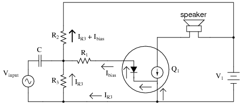
The greater the instantaneous voltage of the input signal, the greater the duty cycle of the output squarewave pulse. If there can be any goal stated of the class D design, it is to avoid active-mode transistor operation. Since the output transistor of a class D amplifier is never in the active mode, only cutoff or saturated, there will be little heat energy dissipated by it. This results in very high power efficiency for the amplifier. Of course, the disadvantage of this strategy is the overwhelming presence of harmonics on the output. Fortunately, since these harmonic frequencies are typically much greater than the frequency of the input signal, these can be filtered out by a low-pass filter with relative ease, resulting in an output more closely resembling the original input signal waveform. Class D technology is typically seen where extremely high power levels and relatively low frequencies are encountered, such as in industrial inverters (devices converting DC into AC power to run motors and other large devices) and high-performance audio amplifiers.
A term you will likely come across in your studies of electronics is something called quiescent, which is a modifier designating the zero input condition of a circuit. Quiescent current, for example, is the amount of current in a circuit with zero input signal voltage applied. Bias voltage in a transistor circuit forces the transistor to operate at a different level of collector current with zero input signal voltage than it would without that bias voltage. Therefore, the amount of bias in an amplifier circuit determines its quiescent values.
In a class A amplifier, the quiescent current should be exactly half of its saturation value (halfway between saturation and cutoff, cutoff by definition being zero). Class B and class C amplifiers have quiescent current values of zero, since these are supposed to be cutoff with no signal applied. Class AB amplifiers have very low quiescent current values, just above cutoff. To illustrate this graphically, a "load line" is sometimes plotted over a transistor's characteristic curves to illustrate its range of operation while connected to a load resistance of specific value shown in Figure below.

Example load line drawn over transistor characteristic curves from Vsupply to saturation current.
A load line is a plot of collector-to-emitter voltage over a range of collector currents. At the lower-right corner of the load line, voltage is at maximum and current is at zero, representing a condition of cutoff. At the upper-left corner of the line, voltage is at zero while current is at a maximum, representing a condition of saturation. Dots marking where the load line intersects the various transistor curves represent realistic operating conditions for those base currents given.
Quiescent operating conditions may be shown on this graph in the form of a single dot along the load line. For a class A amplifier, the quiescent point will be in the middle of the load line as in (Figure below).

Quiescent point (dot) for class A.
In this illustration, the quiescent point happens to fall on the curve representing a base current of 40 µA. If we were to change the load resistance in this circuit to a greater value, it would affect the slope of the load line, since a greater load resistance would limit the maximum collector current at saturation, but would not change the collector-emitter voltage at cutoff. Graphically, the result is a load line with a different upper-left point and the same lower-right point as in (Figure below)

Load line resulting from increased load resistance.
Note how the new load line doesn't intercept the 75 µA curve along its flat portion as before. This is very important to realize because the non-horizontal portion of a characteristic curve represents a condition of saturation. Having the load line intercept the 75 µA curve outside of the curve's horizontal range means that the amplifier will be saturated at that amount of base current. Increasing the load resistor value is what caused the load line to intercept the 75 µA curve at this new point, and it indicates that saturation will occur at a lesser value of base current than before.
With the old, lower-value load resistor in the circuit, a base current of 75 µA would yield a proportional collector current (base current multiplied by β). In the first load line graph, a base current of 75 µA gave a collector current almost twice what was obtained at 40 µA, as the β ratio would predict. However, collector current increases marginally between base currents 75 µA and 40 µA, because the transistor begins to lose sufficient collector-emitter voltage to continue to regulate collector current.
To maintain linear (no-distortion) operation, transistor amplifiers shouldn't be operated at points where the transistor will saturate; that is, where the load line will not potentially fall on the horizontal portion of a collector current curve. We'd have to add a few more curves to the graph in Figure below before we could tell just how far we could "push" this transistor with increased base currents before it saturates.

More base current curves shows saturation detail.
It appears in this graph that the highest-current point on the load line falling on the straight portion of a curve is the point on the 50 µA curve. This new point should be considered the maximum allowable input signal level for class A operation. Also for class A operation, the bias should be set so that the quiescent point is halfway between this new maximum point and cutoff shown in Figure below.

New quiescent point avoids saturation region.
Now that we know a little more about the consequences of different DC bias voltage levels, it is time to investigate practical biasing techniques. So far, I've shown a small DC voltage source (battery) connected in series with the AC input signal to bias the amplifier for whatever desired class of operation. In real life, the connection of a precisely-calibrated battery to the input of an amplifier is simply not practical. Even if it were possible to customize a battery to produce just the right amount of voltage for any given bias requirement, that battery would not remain at its manufactured voltage indefinitely. Once it started to discharge and its output voltage drooped, the amplifier would begin to drift toward class B operation.
Take this circuit, illustrated in the common-emitter section for a SPICE simulation, for instance, in Figure below.

Impractical base battery bias.
That 2.3 volt "Vbias" battery would not be practical to include in a real amplifier circuit. A far more practical method of obtaining bias voltage for this amplifier would be to develop the necessary 2.3 volts using a voltage divider network connected across the 15 volt battery. After all, the 15 volt battery is already there by necessity, and voltage divider circuits are easy to design and build. Let's see how this might look in Figure below.

Voltage divider bias.
If we choose a pair of resistor values for R2 and R3 that will produce 2.3 volts across R3 from a total of 15 volts (such as 8466 Ω for R2 and 1533 Ω for R3), we should have our desired value of 2.3 volts between base and emitter for biasing with no signal input. The only problem is, this circuit configuration places the AC input signal source directly in parallel with R3 of our voltage divider. This is not acceptable, as the AC source will tend to overpower any DC voltage dropped across R3. Parallel components must have the same voltage, so if an AC voltage source is directly connected across one resistor of a DC voltage divider, the AC source will "win" and there will be no DC bias voltage added to the signal.
One way to make this scheme work, although it may not be obvious why it will work, is to place a coupling capacitor between the AC voltage source and the voltage divider as in Figure below.

Coupling capacitor prevents voltage divider bias from flowing into signal generator.
The capacitor forms a high-pass filter between the AC source and the DC voltage divider, passing almost all of the AC signal voltage on to the transistor while blocking all DC voltage from being shorted through the AC signal source. This makes much more sense if you understand the superposition theorem and how it works. According to superposition, any linear, bilateral circuit can be analyzed in a piecemeal fashion by only considering one power source at a time, then algebraically adding the effects of all power sources to find the final result. If we were to separate the capacitor and R2--R3 voltage divider circuit from the rest of the amplifier, it might be easier to understand how this superposition of AC and DC would work.
With only the AC signal source in effect, and a capacitor with an arbitrarily low impedance at signal frequency, almost all the AC voltage appears across R3:

Due to the coupling capacitor's very low impedance at the signal frequency, it behaves much like a piece of wire, thus can be omitted for this step in superposition analysis.
With only the DC source in effect, the capacitor appears to be an open circuit, and thus neither it nor the shorted AC signal source will have any effect on the operation of the R2--R3 voltage divider in Figure below.

The capacitor appears to be an open circuit as far at the DC analysis is concerned
Combining these two separate analyses in Figure below, we get a superposition of (almost) 1.5 volts AC and 2.3 volts DC, ready to be connected to the base of the transistor.

Combined AC and DC circuit.
Enough talk -- its about time for a SPICE simulation of the whole amplifier circuit in Figure below. We will use a capacitor value of 100 µF to obtain an arbitrarily low (0.796 Ω) impedance at 2000 Hz:
 | voltage divider biasing vinput 1 0 sin (0 1.5 2000 0 0) c1 1 5 100u r1 5 2 1k r2 4 5 8466 r3 5 0 1533 q1 3 2 0 mod1 rspkr 3 4 8 v1 4 0 dc 15 .model mod1 npn .tran 0.02m 0.78m .plot tran v(1,0) i(v1) .end |
SPICE simulation of voltage divider bias.
Note the substantial distortion in the output waveform in Figure above. The sine wave is being clipped during most of the input signal's negative half-cycle. This tells us the transistor is entering into cutoff mode when it shouldn't (I'm assuming a goal of class A operation as before). Why is this? This new biasing technique should give us exactly the same amount of DC bias voltage as before, right?
With the capacitor and R2--R3 resistor network unloaded, it will provide exactly 2.3 volts worth of DC bias. However, once we connect this network to the transistor, it is no longer unloaded. Current drawn through the base of the transistor will load the voltage divider, thus reducing the DC bias voltage available for the transistor. Using the diode current source transistor model in Figure below to illustrate, the bias problem becomes evident.
Diode transistor model shows loading of voltage divider.
A voltage divider's output depends not only on the size of its constituent resistors, but also on how much current is being divided away from it through a load. The base-emitter PN junction of the transistor is a load that decreases the DC voltage dropped across R3, due to the fact that the bias current joins with R3's current to go through R2, upsetting the divider ratio formerly set by the resistance values of R2 and R3. To obtain a DC bias voltage of 2.3 volts, the values of R2 and/or R3 must be adjusted to compensate for the effect of base current loading. To increasethe DC voltage dropped across R3, lower the value of R2, raise the value of R3, or both.
 | voltage divider biasing vinput 1 0 sin (0 1.5 2000 0 0) c1 1 5 100u r1 5 2 1k r2 4 5 6k <--- R2 decreased to 6 k r3 5 0 4k <--- R3 increased to 4 k q1 3 2 0 mod1 rspkr 3 4 8 v1 4 0 dc 15 .model mod1 npn .tran 0.02m 0.78m .plot tran v(1,0) i(v1) .end |
No distortion of the output after adjusting R2 and R3.
The new resistor values of 6 kΩ and 4 kΩ (R2 and R3, respectively) in Figure above results in class A waveform reproduction, just the way we wanted.
Biasing calculations
Although transistor switching circuits operate without bias, it is unusual for analog circuits to operate without bias. One of the few examples is "TR One, one transistor radio" TR One, Ch 9 with an amplified AM (amplitude modulation) detector. Note the lack of a bias resistor at the base in that circuit. In this section we look at a few basic bias circuits which can set a selected emitter current IE. Given a desired emitter current IE, what values of bias resistors are required, RB, RE, etc?
Base Bias
The simplest biasing applies a base-bias resistor between the base and a base battery VBB. It is convenient to use the existing VCC supply instead of a new bias supply. An example of an audio amplifier stage using base-biasing is "Crystal radio with one transistor . . . " crystal radio, Ch 9 . Note the resistor from the base to the battery terminal. A similar circuit is shown in Figure below.
Write a KVL (Krichhoff's voltage law) equation about the loop containing the battery, RB, and the VBE diode drop on the transistor in Figure below. Note that we use VBB for the base supply, even though it is actually VCC. If β is large we can make the approximation that IC =IE. For silicon transistors VBE≅0.7V.

Base-bias
Silicon small signal transistors typically have a β in the range of 100-300. Assuming that we have a β=100 transistor, what value of base-bias resistor is required to yield an emitter current of 1mA?
Solving the IE base-bias equation for RB and substituting β, VBB, VBE, and IE yields 930kΩ. The closest standard value is 910kΩ.

What is the the emitter current with a 910kΩ resistor? What is the emitter current if we randomly get a β=300 transistor?

The emitter current is little changed in using the standard value 910kΩ resistor. However, with a change in β from 100 to 300, the emitter current has tripled. This is not acceptable in a power amplifier if we expect the collector voltage to swing from near VCC to near ground. However, for low level signals from micro-volts to a about a volt, the bias point can be centered for a β of square root of (100·300)=173. The bias point will still drift by a considerable amount . However, low level signals will not be clipped.
Base-bias by its self is not suitable for high emitter currents, as used in power amplifiers. The base-biased emitter current is not temperature stable. Thermal run away is the result of high emitter current causing a temperature increase which causes an increase in emitter current, which further increases temperature.
Collector-feedback bias
Variations in bias due to temperature and beta may be reduced by moving the VBB end of the base-bias resistor to the collector as in Figure below. If the emitter current were to increase, the voltage drop across RC increases, decreasing VC, decreasing IB fed back to the base. This, in turn, decreases the emitter current, correcting the original increase.
Write a KVL equation about the loop containing the battery, RC , RB , and the VBE drop. Substitute IC≅IE and IB≅IE/β. Solving for IE yields the IE CFB-bias equation. Solving for IB yields the IB CFB-bias equation.

Collector-feedback bias.
Find the required collector feedback bias resistor for an emitter current of 1 mA, a 4.7K collector load resistor, and a transistor with β=100 . Find the collector voltage VC. It should be approximately midway between VCC and ground.

The closest standard value to the 460k collector feedback bias resistor is 470k. Find the emitter current IE with the 470 K resistor. Recalculate the emitter current for a transistor with β=100 and β=300.

We see that as beta changes from 100 to 300, the emitter current increases from 0.989mA to 1.48mA. This is an improvement over the previous base-bias circuit which had an increase from 1.02mA to 3.07mA. Collector feedback bias is twice as stable as base-bias with respect to beta variation.
Emitter-bias
Inserting a resistor RE in the emitter circuit as in Figure below causes degeneration, also known as negative feedback. This opposes a change in emitter current IE due to temperature changes, resistor tolerances, beta variation, or power supply tolerance. Typical tolerances are as follows: resistor— 5%, beta— 100-300, power supply— 5%. Why might the emitter resistor stabilize a change in current? The polarity of the voltage drop across RE is due to the collector battery VCC. The end of the resistor closest to the (-) battery terminal is (-), the end closest to the (+) terminal it (+). Note that the (-) end of RE is connected via VBB battery and RB to the base. Any increase in current flow through RE will increase the magnitude of negative voltage applied to the base circuit, decreasing the base current, decreasing the emitter current. This decreasing emitter current partially compensates the original increase.
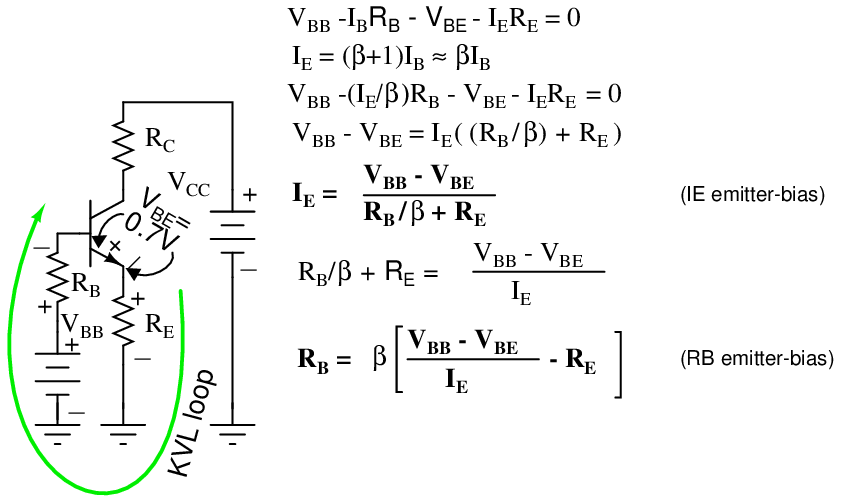
Emitter-bias
Note that base-bias battery VBB is used instead of VCC to bias the base in Figure above. Later we will show that the emitter-bias is more effective with a lower base bias battery. Meanwhile, we write the KVL equation for the loop through the base-emitter circuit, paying attention to the polarities on the components. We substitute IB≅IE/β and solve for emitter current IE. This equation can be solved for RB , equation: RB emitter-bias, Figure above.
Before applying the equations: RB emitter-bias and IE emitter-bias, Figure above, we need to choose values for RC and RE . RC is related to the collector supply VCC and the desired collector current IC which we assume is approximately the emitter current IE. Normally the bias point for VCis set to half of VCC. Though, it could be set higher to compensate for the voltage drop across the emitter resistor RE. The collector current is whatever we require or choose. It could range from micro-Amps to Amps depending on the application and transistor rating. We choose IC = 1mA, typical of a small-signal transistor circuit. We calculate a value for RC and choose a close standard value. An emitter resistor which is 10-50% of the collector load resistor usually works well.

Our first example sets the base-bias supply to high at VBB = VCC = 10V to show why a lower voltage is desirable. Determine the required value of base-bias resistor RB. Choose a standard value resistor. Calculate the emitter current for β=100 and β=300. Compare the stabilization of the current to prior bias circuits.

An 883k resistor was calculated for RB, an 870k chosen. At β=100, IE is 1.01mA.

For β=300 the emitter currents are shown in Table below.
Emitter current comparison for β=100, β=300.
| Bias circuit | IC β=100 | IC β=300 |
|---|---|---|
| base-bias | 1.02mA | 3.07mA |
| collector feedback bias | 0.989mA | 1.48mA |
| emitter-bias, VBB=10V | 1.01mA | 2.76mA |
Table above shows that for VBB = 10V, emitter-bias does not do a very good job of stabilizing the emitter current. The emitter-bias example is better than the previous base-bias example, but, not by much. The key to effective emitter bias is lowering the base supply VBB nearer to the amount of emitter bias.
How much emitter bias do we Have? Rounding, that is emitter current times emitter resistor: IERE = (1mA)(470) = 0.47V. In addition, we need to overcome the VBE = 0.7V. Thus, we need a VBB >(0.47 + 0.7)V or >1.17V. If emitter current deviates, this number will change compared with the fixed base supply VBB,causing a correction to base current IB and emitter current IE. A good value for VB >1.17V is 2V.

The calculated base resistor of 83k is much lower than the previous 883k. We choose 82k from the list of standard values. The emitter currents with the 82k RB for β=100 and β=300 are:

Comparing the emitter currents for emitter-bias with VBB = 2V at β=100 and β=300 to the previous bias circuit examples in Table below, we see considerable improvement at 1.75mA, though, not as good as the 1.48mA of collector feedback.
Emitter current comparison for β=100, β=300.
| Bias circuit | IC β=100 | IC β=300 |
|---|---|---|
| base-bias | 1.02mA | 3.07mA |
| collector feedback bias | 0.989mA | 1.48mA |
| emitter-bias, VBB=10V | 1.01mA | 2.76mA |
| emitter-bias, VBB=2V | 1.01mA | 1.75mA |
How can we improve the performance of emitter-bias? Either increase the emitter resistor RB or decrease the base-bias supply VBB or both. As an example, we double the emitter resistor to the nearest standard value of 910Ω.

The calculated RB = 39k is a standard value resistor. No need to recalculate IE for β = 100. For β = 300, it is:

The performance of the emitter-bias circuit with a 910 emitter resistor is much improved. See Table below.
Emitter current comparison for β=100, β=300.
| Bias circuit | IC β=100 | IC β=300 |
|---|---|---|
| base-bias | 1.02mA | 3.07mA |
| collector feedback bias | 0.989mA | 1.48mA |
| emitter-bias, VBB=10V | 1.01mA | 2.76mA |
| emitter-bias, VBB=2V, RB=470 | 1.01mA | 1.75mA |
| emitter-bias, VBB=2V, RB=910 | 1.00mA | 1.25mA |
As an exercise, rework the emitter-bias example with the base resistor reverted back to 470Ω, and the base-bias supply reduced to 1.5V.

The 33k base resistor is a standard value, emitter current at β = 100 is OK. The emitter current at β = 300 is:

Table below below compares the exercise results 1mA and 1.38mA to the previous examples.
Emitter current comparison for β=100, β=300.
| Bias circuit | IC β=100 | IC β=300 |
|---|---|---|
| base-bias | 1.02mA | 3.07mA |
| collector feedback bias | 0.989mA | 1.48mA |
| emitter-bias, VBB=10V | 1.01mA | 2.76mA |
| emitter-bias, VBB=2V, RB=470 | 1.01mA | 1.75mA |
| emitter-bias, VBB=2V, RB=910 | 1.00mA | 1.25mA |
| emitter-bias, VBB=1.5V, RB=470 | 1.00mA | 1.38mA |
The emitter-bias equations have been repeated in Figure below with the internal emitter resistance included for better accuracy. The internal emitter resistance is the resistance in the emitter circuit contained within the transistor package. This internal resistance REE is significant when the (external) emitter resistor RE is small, or even zero. The value of internal resistance RE is a function of emitter current IE, Table below.
Derivation of REE
REE = KT/IEm where: K=1.38×10⁻²³ watt-sec/oC, Boltzman's constant T= temperature in Kelvins ≅300. IE = emitter current m = varies from 1 to 2 for Silicon REE ≅ 0.026V/IE = 26mV/IE
For reference the 26mV approximation is listed as equation REE in Figure below.

Emitter-bias equations with internal emitter resistance REE included..
The more accurate emitter-bias equations in Figure above may be derived by writing a KVL equation. Alternatively, start with equations IE emitter-bias and RB emitter-bias in Figure previous, substituting RE with REE+RE. The result is equations IE EB and RB EB, respectively in Figure above.
Redo the RB calculation in the previous example emitter-bias with the inclusion of REE and compare the results.

The inclusion of REE in the calculation results in a lower value of the base resistor RB a shown in Table below. It falls below the standard value 82k resistor instead of above it.
Effect of inclusion of REE on calculated RB
| REE? | REE Value |
|---|---|
| Without REE | 83k |
| With REE | 80.4k |
One problem with emitter bias is that a considerable part of the output signal is dropped across the emitter resistor RE (Figure below). This voltage drop across the emitter resistor is in series with the base and of opposite polarity compared with the input signal. (This is similar to a common collector configuration having <1 gain.) This degeneration severely reduces the gain from base to collector. The solution for AC signal amplifiers is to bypass the emitter resistor with a capacitor. This restores the AC gain since the resistor is a short for AC signals. The DC emitter current still experiences degeneration in the emitter resistor, thus, stabilizing the DC current.

Cbypass is required to prevent AC gain reduction.
What value should the bypass capacitor be? That depends on the lowest frequency to be amplified. For radio frequencies Cbpass would be small. For an audio amplifier extending down to 20Hz it will be large. A "rule of thumb" for the bypass capacitor is that the reactance should be 1/10 of the emitter resistance or less. The capacitor should be designed to accommodate the lowest frequency being amplified. The capacitor for an audio amplifier covering 20Hz to 20kHz would be:

Note that the internal emitter resistance REE is not bypassed by the bypass capacitor.
Voltage divider bias
Stable emitter bias requires a low voltage base bias supply, Figure below. The alternative to a base supply VBB is a voltage divider based on the collector supply VCC.

Voltage Divider bias replaces base battery with voltage divider.
The design technique is to first work out an emitter-bias design, Then convert it to the voltage divider bias configuration by using Thevenin's Theorem. [TK1] The steps are shown graphically in Figure below. Draw the voltage divider without assigning values. Break the divider loose from the base. (The base of the transistor is the load.) Apply Thevenin's Theorem to yield a single Thevenin equivalent resistance Rth and voltage source Vth.

Thevenin's Theorem converts voltage divider to single supply Vth and resistance Vth.
The Thevenin equivalent resistance is the resistance from load point (arrow) with the battery (VCC) reduced to 0 (ground). In other words, R1||R2.The Thevenin equivalent voltage is the open circuit voltage (load removed). This calculation is by the voltage divider ratio method. R1 is obtained by eliminating R2 from the pair of equations for Rth and Vth. The equation of R1 is in terms of known quantities Rth, Vth, Vcc. Note that Rth is RB , the bias resistor from the emitter-bias design. The equation for R2 is in terms of R1 and Rth.

Convert this previous emitter-bias example to voltage divider bias.

Emitter-bias example converted to voltage divider bias.
These values were previously selected or calculated for an emitter-bias example
Substituting VCC , VBB , RB yields R1 and R2 for the voltage divider bias configuration.

R1 is a standard value of 220K. The closest standard value for R2 corresponding to 38.8k is 39k. This does not change IE enough for us to calculate it.
Problem: Calculate the bias resistors for the cascode amplifier in Figure below. VB2 is the bias voltage for the common emitter stage. VB1 is a fairly high voltage at 11.5 because we want the common-base stage to hold the emitter at 11.5-0.7=10.8V, about 11V. (It will be 10V after accounting for the voltage drop across RB1 .) That is, the common-base stage is the load, substitute for a resistor, for the common-emitter stage's collector. We desire a 1mA emitter current.

Bias for a cascode amplifier.
Problem: Convert the base bias resistors for the cascode amplifier to voltage divider bias resistors driven by the VCC of 20V.


The final circuit diagram is shown in the "Practical Analog Circuits" chapter, "Class A cascode amplifier . . . " cascode, Ch 9 .
Freddy R Vallenilla R
16.791.006
CAF
No hay comentarios:
Publicar un comentario